S1.pdf - 第5页
Why EUV? - Resolution in Optical Lithography Slide 5 Critical Dimensio n: Depth of focus: k: process parameter NA: numerical aperture : w avele ngth of light KrF -Laser: 248nm ArF -La…
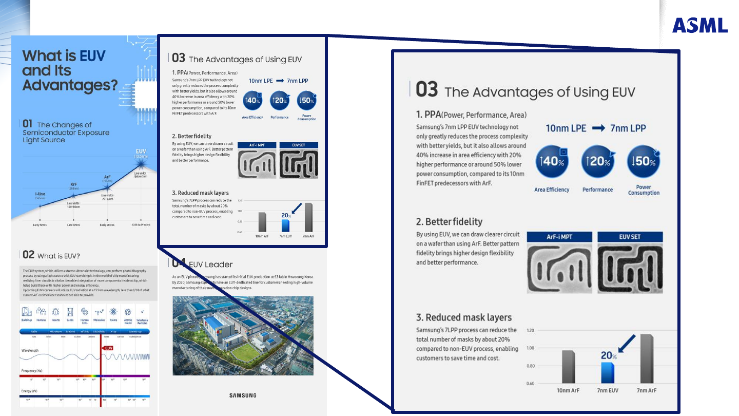
Advantages of EUVL : Samsung Infographic
Lower patterning cost (limiting multiple exposures)
In a full fab, EUV enables higher output
Slide 4
https://news.samsung.com/global/infographic-euv-samsungs-latest-investment-on-developing-next-generation-semiconductor-products
Public
Why EUV? - Resolution in Optical Lithography
Slide 5
Critical Dimension:
Depth of focus:
k: process parameter
NA: numerical aperture
: wavelength of light
KrF-Laser: 248nm
ArF-Laser: 193 nm
ArF-Laser (immersion): 193 nm
EUV sources: 13.5 nm
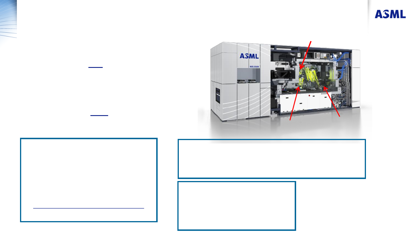
EUV source
Wafer stage
Reticle stage
theoretical limit (air): NA=1
practical limit: NA=0.9
theoretical limit (immersion):NA ≈ n (~1.7)
k
1
is process parameter
traditionally: >0.75
typically: 0.3 – 0.4
theoretical limit: 0.25
Public
Slide 6
EUV development has progressed over 30 years
from NGL to HVM insertion
’84
1
st
lithography
(LLNL, Bell Labs,
Japan)
USA
40 nm hp
70 nm
L&S
Japan
80 nm
160 nm
NL
28 nm
Lines and spaces
USA
5 mm
ASML starts
EUVL research
program
ASML ships 1
st
pre-production NA
0.25 system
NXE:3100
ASML ships 1
st
NA 0.33 system
NXE:3300B
NL
13 nm L/S
ASML ships 1
st
HVM NA0.33 system
NXE:3400B
NL
7 nm and 5 nm
node structures
’85 ’86 ’87 ’88 ’89 ’90 ’91 ’92 ’93 ’94 ’95 ’96 ’97 ’98 ’99 ’00 ’01 ’02 ’03 ’04 ’05 ’06 ’07 ’08 ’09 ’10 ’11 ’12 ‘13 ’14 ’15 ’16 ’17 ’18
NL
19 nm
Lines and spaces
ASML ships
2 alpha demo tools:
IMEC (Belgium) and
CNSE (USA)
USANL NL NL
Public