S1.pdf - 第7页
1 10 100 1, 000 1985 1990 1995 2000 2005 2010 2015 2020 2025 High-NA EUV targets <7nm resolution Relative impro vemen t:5X over ArFi, 40% over 0.33 NA EUV Year of introduction Slide 7 13 .5, EUV 193 , ArF 248 , KrF 36…
Slide 6
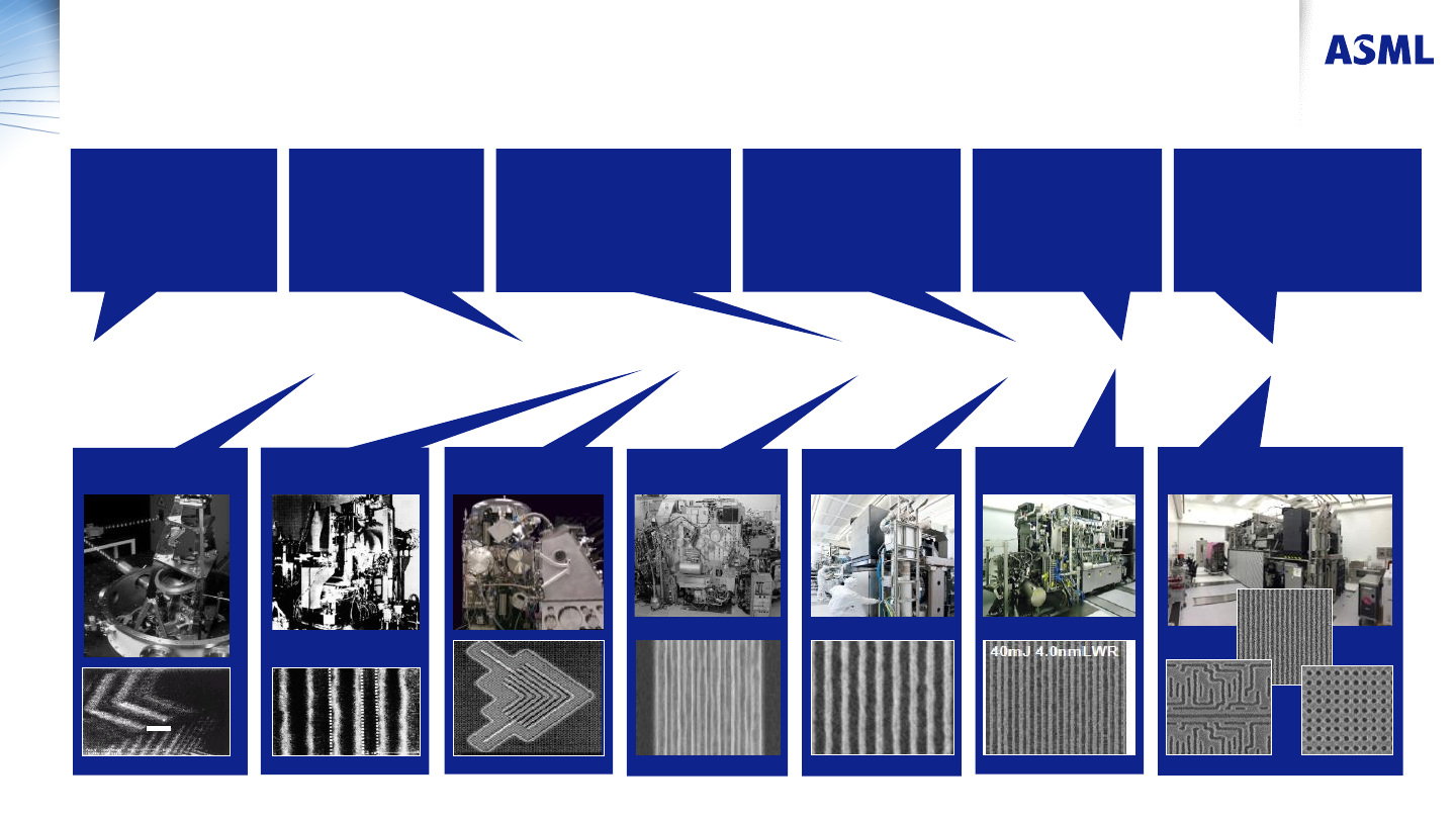
EUV development has progressed over 30 years
from NGL to HVM insertion
’84
1
st
lithography
(LLNL, Bell Labs,
Japan)
USA
40 nm hp
70 nm
L&S
Japan
80 nm
160 nm
NL
28 nm
Lines and spaces
USA
5 mm
ASML starts
EUVL research
program
ASML ships 1
st
pre-production NA
0.25 system
NXE:3100
ASML ships 1
st
NA 0.33 system
NXE:3300B
NL
13 nm L/S
ASML ships 1
st
HVM NA0.33 system
NXE:3400B
NL
7 nm and 5 nm
node structures
’85 ’86 ’87 ’88 ’89 ’90 ’91 ’92 ’93 ’94 ’95 ’96 ’97 ’98 ’99 ’00 ’01 ’02 ’03 ’04 ’05 ’06 ’07 ’08 ’09 ’10 ’11 ’12 ‘13 ’14 ’15 ’16 ’17 ’18
NL
19 nm
Lines and spaces
ASML ships
2 alpha demo tools:
IMEC (Belgium) and
CNSE (USA)
USANL NL NL
Public
1
10
100
1,000
1985 1990 1995 2000 2005 2010 2015 2020 2025
High-NA EUV targets <7nm resolution
Relative improvement:5X over ArFi, 40% over 0.33 NA EUV
Year of introduction
Slide 7
13.5, EUV
193, ArF
248, KrF
365, i-line
436, g-line
>10x
NA+67%
Resolution, nm
= k
1
x Wavelength / NA
Wavelength, nm
>2021
i-Line 365 nm
KrF 248 nm
ArFi 193 nm
ArF 193 nm
EUV 13.5 nm
Production systems
Development systems
XT:1400
NXT:1950i
NXE:3400
High-NA
g-Line 436 nm
NA+45%
Public
Slide 8
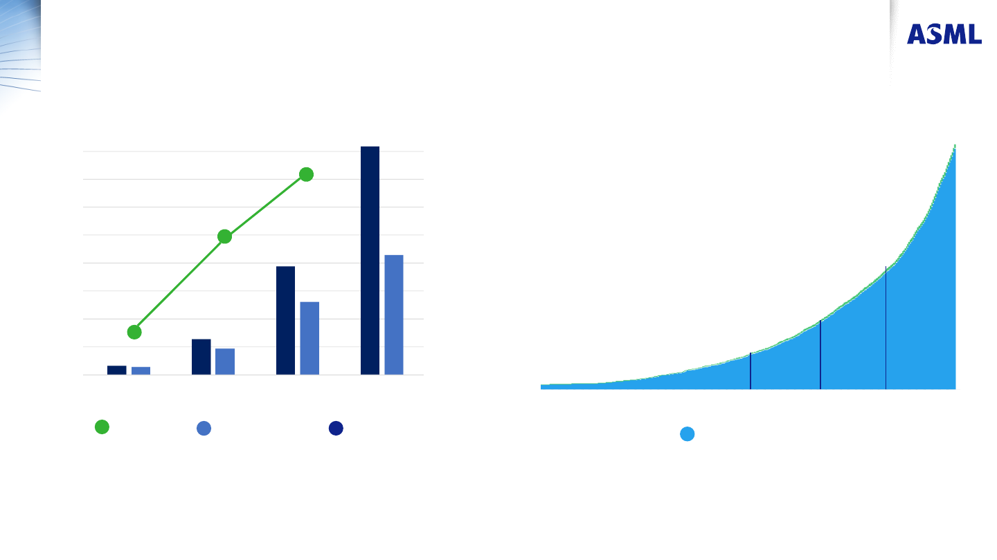
EUV is being ramped up quickly now
Since Jan 2018, EUV systems have run more
wafers (2.5M) than 2011-2017 combined
2013
EUV yearly shipped and cumulative capacity [10
3
wafers/day]
NXE:3400B installed base stands at 38 (per
Q2 2019), cumulative EUV wafer capacity
will approach 10
8
wafers per year by 2020
2020
2019
2018
2017
0
5
10
15
20
30
35
40
27
10
#systems
in fabs
Capacity (wpd)
Cumulative
capacity (wpd)
0
5
10
15
20
25
30
35
40
Worldwide installed base (3400B)
4.5M
2019
2018
2017
2016
2015
2014
2M
1.1M
0.6M
Cumulative wafer count
38
(per Q219)
25
Installed base NXE:3400B
Cumulative EUV wafer count
Public