4M184002w_F8S.pdf - 第309页
4OM-1840 5-1-10 1604-001 (2) Missing Components on PCB (2-1) Situational Grasp of Error Generation The following three symptoms can be assumed regarding why some components are missing. • Some components were lifted up d…
4OM-1840
5-1-91604-001
(1-3) Positional or Angular Deviation in Process D or E
When a positional deviation is not generated on the double-faced tape, it
indicates that positional and angular deviations occur in Process D or E.
As a symptom at this time
•
The component is dislocated right after it is placed.
•
The component is dislocated during operation subsequent to the placement.
•
The component is dislocated during PCB discharge operation subsequent
to the placement.
shape of the component, the condition of the PCB, or the condition of solder
paste or glue.
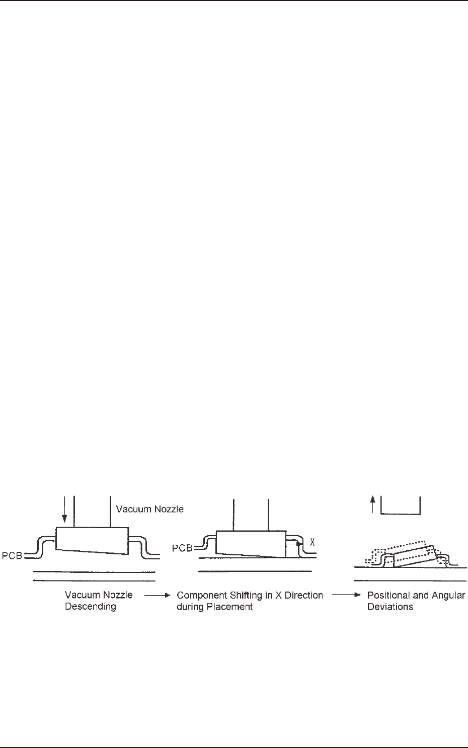
F4E8 is an example, which shows that a component is dislocated right after
it is placed due to the upper and lower surfaces of the component not parallel
to each other.
moment when the lower surface touches the PCB during placement.
This leads to the positional and angular deviations of the component
placement.
When this type of component is used, this failure may be avoided by slowing
down the placement speed or slightly increasing the nozzle descent level for
the placement.
Some components may be dislocated easily during the backup base
movement or a PCB discharge operation after they are placed.
The factor may be weak holding power of solder paste or glue or imperfect
It is required to check these conditions and take individual countermeasures.
Easily-Dislocated Component during Placement (Example 2) F4E8
3.1 Cause and Remedy of Placement Errors
4OM-1840
5-1-101604-001
(2) Missing Components on PCB
(2-1) Situational Grasp of Error Generation
The following three symptoms can be assumed regarding why some
components are missing.
•
Some components were lifted up during placement.
•
Some components sprang out due to vibrating PCB or vacuum break
during placement.
•
A component sprang out while the PCB is being discharged after
placement.
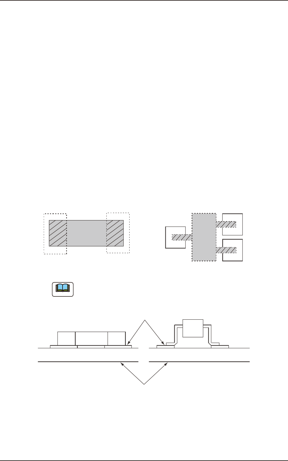
The smaller the touch area with the PCB (solder paste) is in comparison with
the component size, the more frequently this type of failure occurs.
This applies commonly to these symptoms.
As shown in Fig. 4E9, power enough to hold a component will be given
when square components (resistors, capacitors, etc.) are used. However,
the above symptoms may appear more frequently when leaded components
(transistors, diodes, etc.) are handled because of the small touch areas.
Square Component
Leaded Component
Shadowed are the touch areas between the components
and the solder paste.
Solder Paste
PCB
Note
F4E9
3.1 Cause and Remedy of Placement Errors
4OM-1840
5-1-111604-001
(2-2) Machine-Based Factors
Shown below are the assumable main factors based on the machine.
When trouble occurs in some of the components (the components of the
same type that have been used in the past actual production), check for the
following factors.
•
Worn, Clogged, or Dirty Vacuum Nozzle
•
Vacuum Nozzle Up/Down Movement Error
•
Flow Rate of Broken Vacuum and Performance Error
•
Improper Placement Height Level
•
Imperfect Holding Power for Z Clamping
•
Dirt and/or Nicks on Linear Measure Sensor
(3) Other Factors
The factors other than the machine-based ones are assumed to be the shape
of the component, the condition of the PCB, or the condition of solder paste
or glue.
The factors are shown in the table below.
Check each item and take measures if necessary.
If no quick improvement can be made due to the condition of the PCB or
solder paste, failures can be avoided by slowing down the speed of the
component placement or the PCB transfer.
Component
A foreign substance exists on the upper surface of a
component and adheres to the vacuum nozzle.
There is a protruding portion on the upper surface
of a component, causing the lower surface of the
vacuum nozzle to wear out and an error during the
teaching operation through component recognition
lighting.
Oil or mold lubricant adheres to the lower surface of
a component.
PCB
Some PCBs vibrate during component placement
because the warpage is great.
in shape.
Glue
Shortage of Applied Glue
Solder Paste
Shortage of Applied Solder Paste
Shortage of Adhesion
T4E2
3.1 Cause and Remedy of Placement Errors