00198382-03_UM_SIPLACE-CA4-V2_EN.pdf - 第136页
3 Technical data and assemblies I nstruction manual SIPLACE CA4 V 2 3.7 PCB conveyor system From software version 713.0 Edition 12/20 19 136 3.7.7 PCB warp age fo r single lane and dual lane conveyor 3.7.7.1 PCB warp age…

Instruction manual SIPLACE CA4 V2 3 Technical data and assemblies
From software version 713.0 Edition 12/2019 3.7 PCB conveyor system
135
3.7.6.2 Panel lane and wafer lane conveyor
3
Panel lane conveyor Wafer lane conveyor
Vacuum tooling
L330 x W315
Vacuum tooling
L625 x W615
Vacuum tooling DM 300
Workpiece carrier dimensions
Width x length to
330 mm x 330 mm
to
650 mm x 685
mm
*a
--
Diameter -- -- to 300 mm
*b
Automatic electrical width adjustment Standard
Workpiece thickness
Vacuum tooling L330 x W315
Vacuum tooling L625 x W615
Vacuum tooling DM 300 ST 0.55
Vacuum tooling DM 300 ST 1,25
0.3 mm to 4.5 mm
0.3 mm to 4.5 mm
--
--
--
--
0.55 mm
1.25 mm
Workpiece carrier warpage See page 138
Workpiece carrier weight
*c
Cycle time 60 min / 3 years service life
Cycle time 10 min / 3 years service life
Cycle time 0,25 min / 3 years service life
Max. 10.0 kg
Max. 6.0 kg
*d
Max. 3.0 kg
d
Max. 10.0 kg
Max. 6.0 kg
d
Max. 3.0 kg
d
--
--
Max. 3.0 kg
d
Space on the workpiece carrier underside 0.0 mm
Workpiece carrier transportation height
Option
Standard:
Option SMEMA
900 mm
930 mm
950 mm
Type of interface SMEMA or The Hermes Standard
Component-free PCB handling edge 3 mm
Workpiece carrier changeover time < 1.5 seconds
*)a With long board option (LBO)
*)b In the case of rectangular workpiece carriers, 330 mm x 330 mm is possible
*)c The workpiece weight value refers to the weight of the workpiece plus the weight of the components.
*)d Shorter cycle times could lead to reduced service life or an increased need for spare parts.
3 Technical data and assemblies Instruction manual SIPLACE CA4 V2
3.7 PCB conveyor system From software version 713.0 Edition 12/2019
136
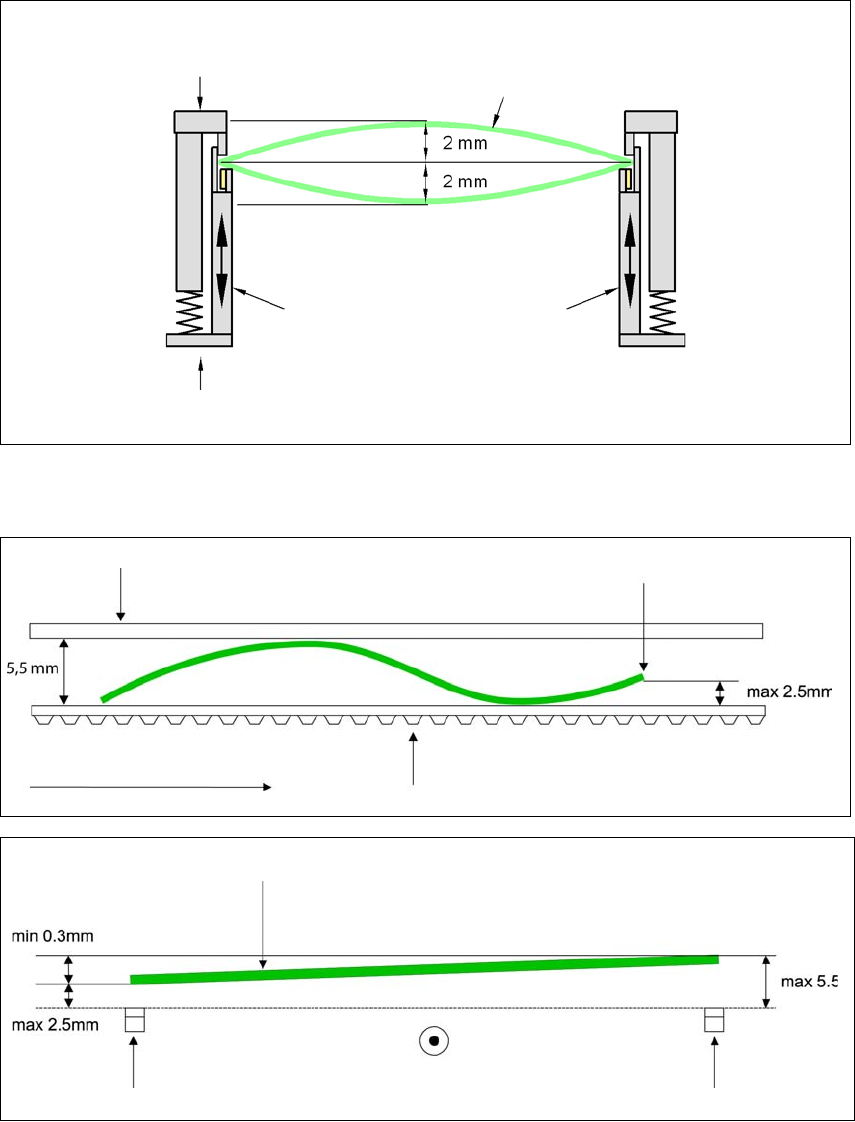
3.7.7 PCB warpage for single lane and dual lane conveyor
3.7.7.1 PCB warpage on the conveyor
PCB warpage across the direction of travel max. 1 % of the PCB diagonal, but not exceeding 2 mm
3
PCB warpage in the direction of conveyor + PCB thickness < 5.5 mm. Bending up of board edge
max. 2.5 mm.
3
3
Fixed clamped edge
Movable clamping device
Printed circuit board
Conveyor side
Fixed clamped edge
Conveyor belt
PCB conveyor direction
Front board edge
Front board edge
Right conveyor belt
Left conveyor belt
PCB conveyor direction
Instruction manual SIPLACE CA4 V2 3 Technical data and assemblies
From software version 713.0 Edition 12/2019 3.7 PCB conveyor system
137
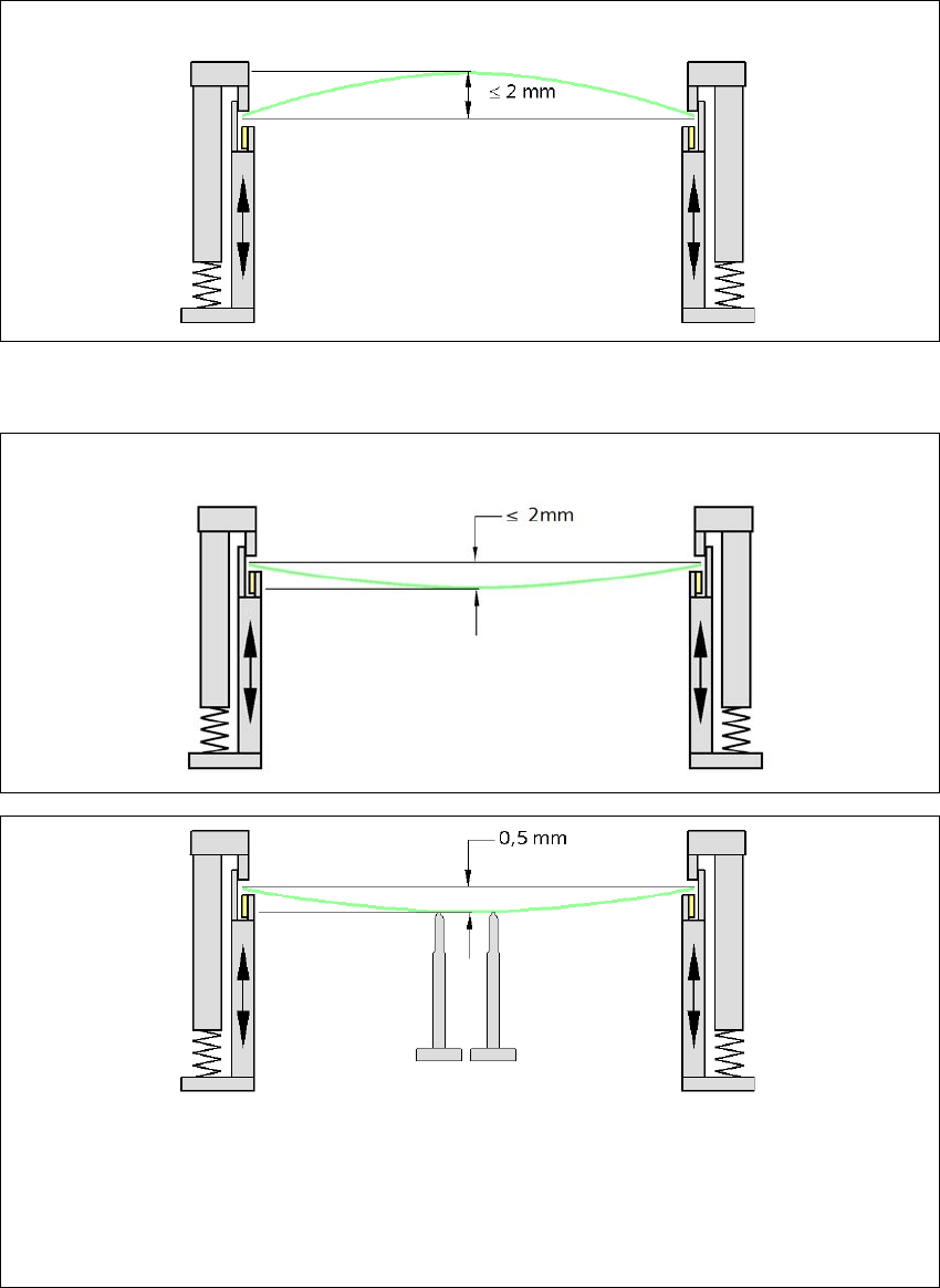
3.7.7.2 PCB warpage during placement
3
3
Changes in the surface position are automatically applied by the functions for learning the height.
3
3
PCB warpage up, max. 2.5 mm
PCB warpage down, max. 2.5 mm
PCB support
To avoid impairing the placement quality and speed, we recommend using a PCB support e.g.
Smart Pin Support so that the PCB warpage downwards does not exceed 0.5 mm.