Oxford-100-Manual.pdf - 第272页
All OIPT Systems Oxford Instruments Plasma Technology System Manual RFOUT TO DC BIAS CIRCUIT C2 PADDING CAPACITORS C1 TYPICAL MATCHING COMPONENTS (LAYOUT 1) RF IN ~------------------------------------------------- I I I …
System
Manual
Oxford
Instruments
Plasma
Technology
All
OIPT Systems
Note
that
shows an
AMU
control
panel
with
control
facilities
for
two
AMUs. The
left-hand
side controls are
for
AMU1 and
the
right-hand
side controls are
for
AMU2. The
LCD
displays
are switched using
the
DISPLAY
SELECTOR
switch
as
shown
in
the
following
table.
DISPLAY SELECTOR LCD 1 (UPPER)
LCD 2 (LOWER)
POSITION
1
AMU
1
C1
POSITION
AMU
1
C2
POSITION
2
RF
1 FORWARD
POWER
RF
1
REFLECTED
POWER
3
RF
1
SETPOINT
RF
1 Hilla
4
RF
2 FORWARD
POWER
RF
2
REFLECTED
POWER
5
RF
2
SETPOINT
SPARE
6
AMU
2
C1
POSITION
AMU
2
C2
POSITION
For a circuit
diagram
of
the
AMU
control
panel.
refer
to
drawing
94-SEOOC23249.
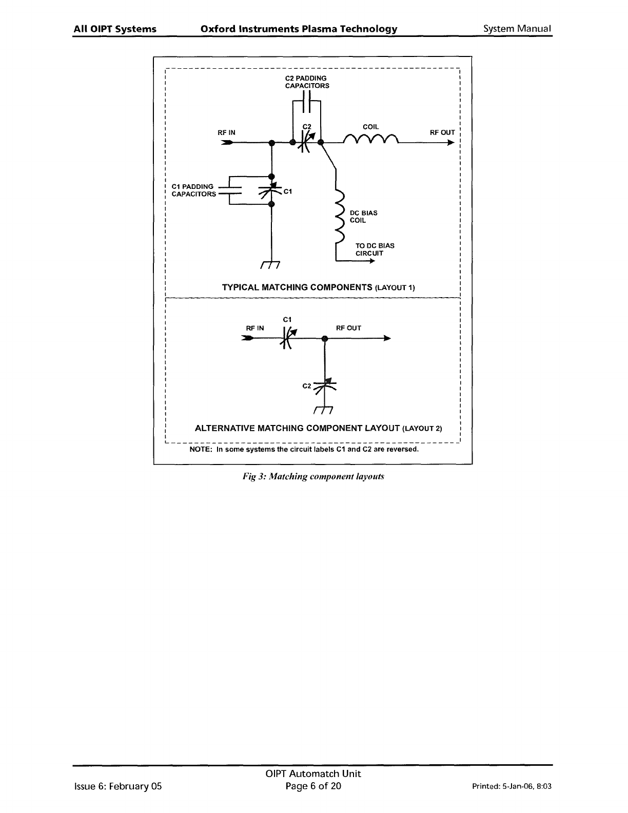
2.3
Matching
component
layouts
The
layout
of
the
matching
components depends
on
the
device
to
be matched
to
the
RF
Generator
to
ensure
maximum
power
transfer. Typical layouts
of
the
components are shown
in Fig
3.
Note
that
in
the
typical layout,
padding
capacitors can be added in parallel
with
C1
and
C2
to
modify
their
capacitance ranges. Refer
to
sub-section 6.3 (page 19)
for
details.
Printed: 5-Jan-06, 8:03
OIPT
Automatch
Unit
Page 5
of
20
Issue
6:
February
05
All
OIPT
Systems
Oxford
Instruments
Plasma
Technology
System
Manual
RFOUT
TO
DC
BIAS
CIRCUIT
C2 PADDING
CAPACITORS
C1
TYPICAL MATCHING COMPONENTS (LAYOUT 1)
RF
IN
~-------------------------------------------------
I
I
I
I
I
I
I
I
C1
PADDING
: CAPACITORS
I
I
I
I
I
I
I
I
I
I
I
I
I
I
I
I
I
RFOUT
C2
C1
RFIN
I
I
I
I
I
I
I
I
I
I
I
I
I
I
I
I
I
I
I
I
I
I
: ALTERNATIVE MATCHING COMPONENT LAYOUT (LAYOUT 2) I
I I
L
1
NOTE: In
some
systems
the
circuit
labels
C1
and
C2 are reversed.
Fig
3:
Matching component layouts
Issue
6:
February 05
OIPT
Automatch
Unit
Page 6
of
20
Printed: 5-Jan-06. 8:03
System Manual
Oxford
Instruments
Plasma
Technology
All
OIPT Systems
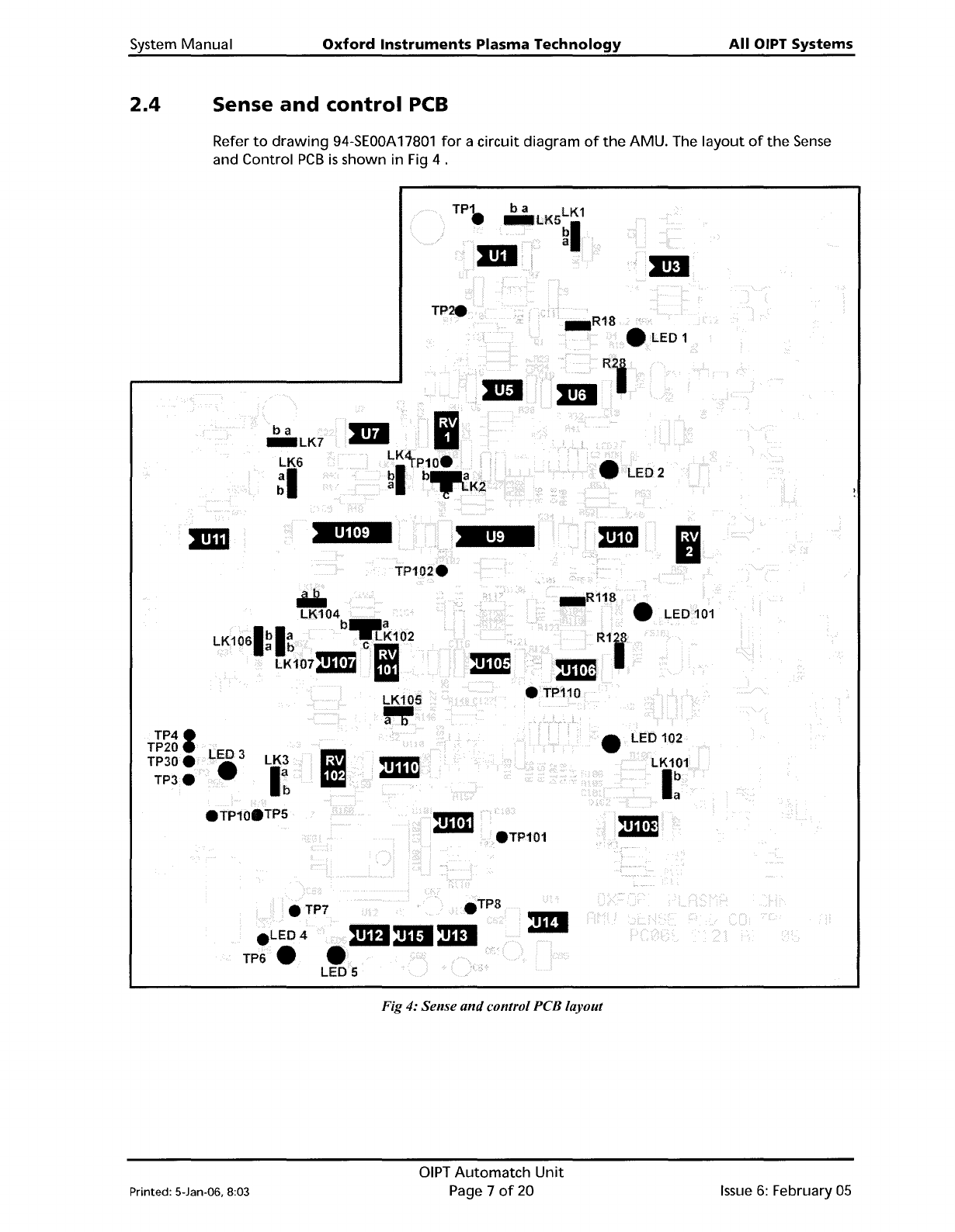
2.4
Sense
and
control
PCB
Refer
to
drawing
94-SEOOA
17801
for
a circuit diagram
of
the
AMU. The
layout
of
the
Sense
and Control
PCB
is
shown in Fig 4 .
TP.
..1.ED1
ba
_LK7
LK6
~I
2
Ii
Iii.
LK104
b_a
LK1061bla
-.LK102
a b
em
LK107211'!1
Iii
LK105
".
• LED 102
TP41
TP20
TP30e
TP3e
LED 3
•
LK3
I~
• LED
101
eTP101
4i\mDmI:mI
LED 5
eTP7
e
LED4
TP6.
Fig 4: Sense
and
control PCB layout
Printed: 5-Jan-06, 8:03
DIPT
Automatch
Unit
Page 7
of
20
Issue
6:
February
05