IPC-T-50F_.pdf.pdf - 第18页
Circuit 21.0213 A number of electrical elements and devices that have been interconnected to perform a desired electrical function. Circuit Card 60.0214 see ‘ ‘Printed Board.’ ’ Circuitry Layer 22.0215 A layer of a print…
Chamfer (Drill) 51.0193
The angle at the end of a drill shank.
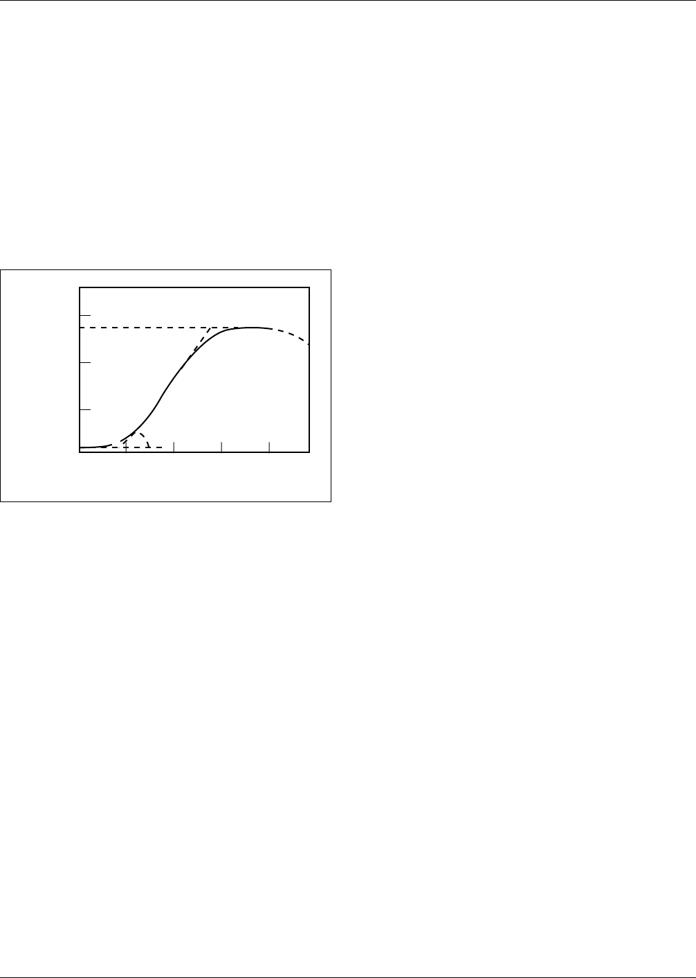
Characteristic Curve 24.1347
A plot of photographic product optical-density data versus
the logarithm of the exposure used to characterize the
response of the material to exposure and development. (See
Figure C-2.)
Characteristic Impedance 21.0194
The resistance of a parallel conductor structure to the flow
of alternating current (AC), usually applied to high speed
circuits, and normally consisting of a constant value over a
wide range of frequencies.
Check List 94.1219
A compilation of the specified criteria that may be evalu-
ated during an audit or inspection.
Check Plot 94.0195
An interim drawing used for graphical data verification.
Check Sheet 94.0196
A form that is used for data collection.
Chelate Compound 76.0197
A compound in which metal is contained as an integral part
of a ring structure.
Chelating Agent 76.0198
A compound capable of forming a chelate compound with
a metal ion.
Chemical Conversion Coating 57.0199
A protective coating produced by the chemical reaction of
a metal with a chemical solution.
Chemical Vapor Deposition 45.0202
The deposition of a film onto the surface of a substrate by
the chemical reduction of a vapor on contact with the base
material.
Chemical Wire Stripping 37.0203
The process of removing insulation from wire using chemi-
cal compounds.
Chemically-Deposited Printed Circuit 50.0201
see ‘‘Additive Process.’’
Chemically-Deposited Printed Wiring 50.0200
see ‘‘Additive Process.’’
Chemisorption 74.1348
The formation of bonds between the surface molecules of
a metal, or other material of high surface energy, and
another gas or liquid substance in contact with it.
Chessman 74.0204
A disk, knob or lever used to manually control the position
of a bonding tool with respect to land.
Chip 35.0205
see ‘‘Die.’’
Chip Carrier 33.0208
A low-profile, usually square, surface-mount component
semiconductor package whose die cavity or die mounting
area is as large fraction of the package size and whose
external connections are usually on all four sides of the
package. (It may be leaded or leadless.)
Chip-and-Wire 74.0206
An assembly method that uses discrete wires to intercon-
nect back-bonding die to lands, lead frames, etc.
Chip-on-Board (COB) 86.0207
A printed board assembly technology that places unpack-
aged semiconductor dice and interconnects them by wire
bonding or similar attachment techniques. Silicon area den-
sity is usually less than of the printed board.
Chipped Point 51.0209
A condition whereby the amount of chips on the leading
edge of a drill point exceeds an allowable value.
Chisel 74.0210
A tool used for wedge and ultrasonic bonding.
Chisel-Edge Angle 51.0211
The angle between the leading cutting edge and the inter-
section of the primary and secondary relief facets of a drill
point.
Chopped Bond 74.0212
A bond with excessive deformation such that the strength
of the bond is greatly reduced.
IPC-I-002331
Figure C–2 Typical Characteristic Curve
log E
30
D
20
10
f
1
D
Density
00 10 20 30 40
B
A
C
F
P
θ
June 1996 IPC-T-50F
13
Circuit 21.0213
A number of electrical elements and devices that have been
interconnected to perform a desired electrical function.
Circuit Card 60.0214
see ‘‘Printed Board.’’
Circuitry Layer 22.0215
A layer of a printed board containing conductors, including
ground and voltage planes.
Circumferential Separation 96.1349
A crack or void in the plating extending around the entire
circumference of as plated through hole, a solder fillet
around lead wire or eyelet, or the interface between a sol-
der fillet and a land.
Circumferential Thermodes 74.1734
A contact tool used for inner-lead and outer-lead gang
bonding.
Clad (adj.) 55.1350
A condition of the base material to which a relatively-thin
layer or sheet of metal foil has been bonded to one or both
of its sides, e.g. ‘‘a metal-clad base material.’’
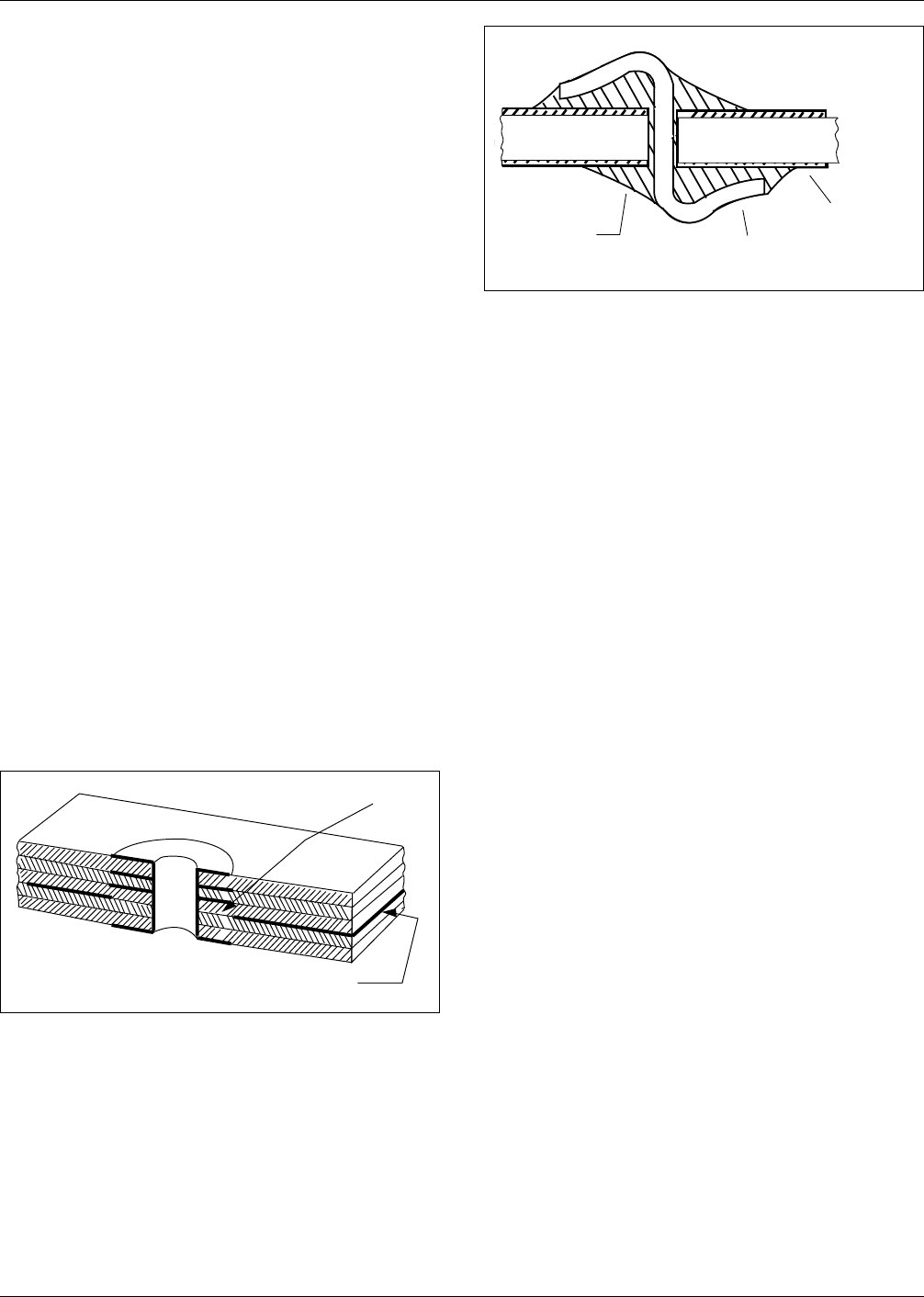
Clearance Hole 22.1811
A hole in a conductive pattern that is larger than, and
coaxial with a hole in the base material of a printed board.
(See Figure C-3.)
Clinched Lead 72.1351
A component lead that is inserted through a hole in a
printed board and is then formed in order to retain the
component in place and in order to make metal-to-metal
contact with a land prior to soldering. (See also ‘‘Partially-
Clinched Lead.’’)
Clinched-Wire Interfacial Connection 72.0217
see ‘‘Clinched-Wire Through Connection.’’
Clinched-Wire Through Connection 72.1352
A connection made by a bare wire that has been passed
through a hole in a printed board and subsequently formed
(clinched) and soldered to the conductive pattern on each
side of the board. (See Figure C-4.)
Closed-Entry Contact 37.0218
A type of female connector contact that prevents the entry
of an oversized mating part. (See also ‘‘Open-Entry Con-
tact.’’)
Co-Firing 56.0219
The simultaneous processing of thick-film circuit elements
during one firing cycle.
Coaxial Cable 37.0220
A cable in the form of a central wire surrounded by a con-
ductor tubing or sheathing that serves as a shield and
return.
Coefficient of Thermal Expansion (CTE) 40.0221
The linear dimensional change of a material per unit
change in temperature. (See also ‘‘Thermal Expansion Mis-
match.’’)
Cohesion Failure 96.0222
The rupture of an adhesive bond such that the separation
appears to be within the adhesive.
Coined Lead 22.0223
The end of a round lead that has been formed to have par-
allel surfaces that approximate the shape of a ribbon lead.
Cold Hand Cleaning 76.0224
Cleaning with a soft brush and rinsing in a small open tank
of chlorinated solvent or isopropanol. (Propan-2-01.)
Cold Machine Cleaning 76.0225
Cleaning with a chlorinated solvent and an inline brush or
wave cleaner.
IPC-I-001035
Figure C–3 Clearance hole
Conductive Pattern
Clearance Hole
IPC-I-001027
Figure C–4 Clinched-wire through connection
Solder
Lead
Conductive
Pattern
▼
▼
▼
IPC-T-50F June 1996
14

Cold Solder Connection 97.0226
A solder connection that exhibits poor wetting, and that is
characterized by a greyish porous appearance. (This is due
to excessive impurities in the solder, inadequate cleaning
prior to soldering, and/or the insufficient application of heat
during the soldering process.) (See alse ‘‘Rosin Solder
Connection.’’)
Color Temperature 24.1355
A measure of the energy distribution over the visible spec-
tral range of a light source with a continuous spectrum,
expressed in degrees Kelvin (K). (See also ‘‘Effective
Color Temperature.’’)
Comb Pattern 22.0227
A set of interdigitated comblike arrays of uniformly-spaced
conductors.
Comment Record 25.0228
A record that provides, or refers to, additional descriptive
material that further clarifies the control of a data set.
Common Cause 91.0229
A source of variation that affects all the individual values
of the output of a process.
Compensated Artwork 24.0230
Production master or artwork data that has been enlarged
or reduced in order to meet the needs of subsequent pro-
cessing requirements.
Compensation Circuit 21.0231
An electrical circuit that alters the functioning of another
circuit to which it is applied to achieve desired perfor-
mance.
Compiler 11.0232
A software module that analyzes and converts programs
from a high-level language to binary machine codes.
Complex Ion 76.0233
An ion composed of two or more ions or radicals that are
capable of an independent existence.
Compliant Bond 74.0235
A bond that uses an elastically- and/or plastically-
deformable member to impart the required energy to the
lead.
Component 30.0236
An individual part or combination of parts that, when
together, perform a design function(s). (See also ‘‘Discrete
Component.’’)
Component Density 22.0237
The quantity of components on a unit area of printed board.
Component Hole 20.0238
A hole that is used for the attachment and/or electrical con-
nection of component terminations, including pins and
wires, to a printed board.
Component Lead 30.1356
The solid or stranded wire or formed conductor that
extends from a component to serve as a mechanical or
electrical connector, or both. (See also ‘‘Component Pin.’’)
Component Mounting 70.0239
The act of attaching components to a printed board, the
manner in which they are attached, or both.
Component Mounting Orientation 22.1357
The direction in which the components on a printed board
or other assembly are lined up electrically with respect to
the polarity of polarized components, with respect to one
another, and/or with respect to the board outline.
Component Pin 30.0240
A component lead that is not readily formable without
being damaged. (See also ‘‘Component Lead.’’)
Component Side 22.0241
see Primary Side .
Component Thermal Masses 30.1735
The ability of a part to absorb or retain heat energy, usu-
ally relative to its overall size and weight.
Composite (Phototool) 24.0242
A photograph that consists of a combination two separate
(aligned) images.
Composite Record 25.1358
A collection of records that make up an electrical pattern
that is used repeatedly in a design. (The definition and
relationship of such records are covered and referred to as
‘‘subroutine definition’’ and ‘‘subroutine definition call.’’)
Composite Test Pattern (CTP) 24.1792
A grouping of individual test patterns into specific arrange-
ments, to reflect control and precision capability of a manu-
facturer or manufacturing process.
Compression Seal 36.0243
A tight joint made between an component package and its
leads that is formed as heated metal cools and shrinks
around a glass insulator.
Computer Numerical Control (CNC) 11.0244
A system that utilizes a computer and software as the pri-
mary numerical control technique. (See also ‘‘Numerical
Control.’’)
June 1996 IPC-T-50F
15