IPC-T-50F_.pdf.pdf - 第49页
N Nail Heading 51.0794 The flared condition of copper on an inner conductive layer of a multilayer printed board that is caused by hole-drilling. (See Figure N-1.) Nail 92.0792 see ‘ ‘Probe, T est.’ ’ Nailhead Bond 74.079…
Mounting Hole 20.0779
A hole that is used for the mechanical support of a printed
board or for the mechanical attachment of components to a
printed board.
Muffle 75.0780
An enclosure that is located between the heating elements
and the parts being processed that contains the atmosphere
required for the reflow soldering process.
Multi-Vari 91.0781
A nonmathematical method for determining the sources of
variation.
Multichip Integrated Circuit 86.0782
see ‘‘Multichip Module.’’
Multichip Microcircuit 86.0783
see ‘‘Multichip Module.’’
Multichip Module (MCM) 86.0784
A microcircuit module consisting primarily of closely-
spaced unpackaged semiconductor dice or chip scale pack-
ages, that have a silicon area density of usually more than
of the module area.
Multilayer Carrier Tape 36.0785
Carrier tape with two or more conductor layers.
Multilayer Printed Board 60.1227
The general term for a printed board that consist of rigid or
flexible insulation materials and three or more alternate
printed wiring and/or printed circuit layers that have been
bonded together and electrically interconnected.
Multilayer Printed Circuit Board 60.0786
A multilayer printed board with two or more printed circuit
layers.
Multilayer Printed Circuit Board Assembly 80.0787
An assembly that uses a multilayer printed circuit board for
component mounting and interconnecting purposes.
Multilayer Printed Wiring Board 60.0788
A multilayer printed board with only printed wiring for its
conductive layers.
Multilayer Printed Wiring Board Assembly 80.0789
An assembly that uses a multilayer printed wiring board for
component mounting and interconnecting purposes.
Multilevel Experiment 91.0790
The evaluation of a small number of factors at a large
number of levels.
Multiple Image Production Master 24.1643
A production master having at least two1:1scale patterns
Multiple Indications 91.0791
An anomaly that is detected and reported more than once.
Multiple Pattern 24.1645
The arrangement of two or more1:1scale patterns con-
tained within the size of one panel.
Multiple Printed Panel 50.1646
A printed panel in which one of more patterns occur two
or more times, processed as a single unit and subsequently
divided.
IPC-I-001207
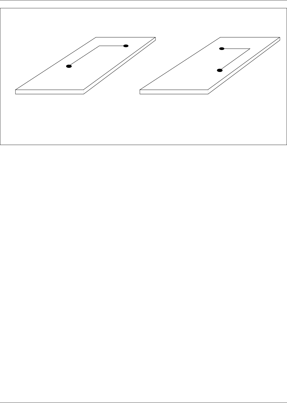
Figure M–2 Mirrored and right-reading patterns
1 2 3 4
Primary Side Viewing
Right Reading Pattern Mirrored Pattern
NOTE: Phototooling emulsion for the right reading pattern is by definition the same as for the
mirrored pattern. That is, both are either emulsion up or both emulsion down.
1 2 3 4
Primary Side Viewing
IPC-T-50F June 1996
44
N
Nail Heading 51.0794
The flared condition of copper on an inner conductive layer
of a multilayer printed board that is caused by hole-drilling.
(See Figure N-1.)
Nail 92.0792
see ‘‘Probe, Test.’’
Nailhead Bond 74.0793
see ‘‘Ball Bond.’’
Near-End Crosstalk 21.0795
see ‘‘Backward Crosstalk.’’
Neckbread 74.0796
A break in a bond immediately above a ball bond.
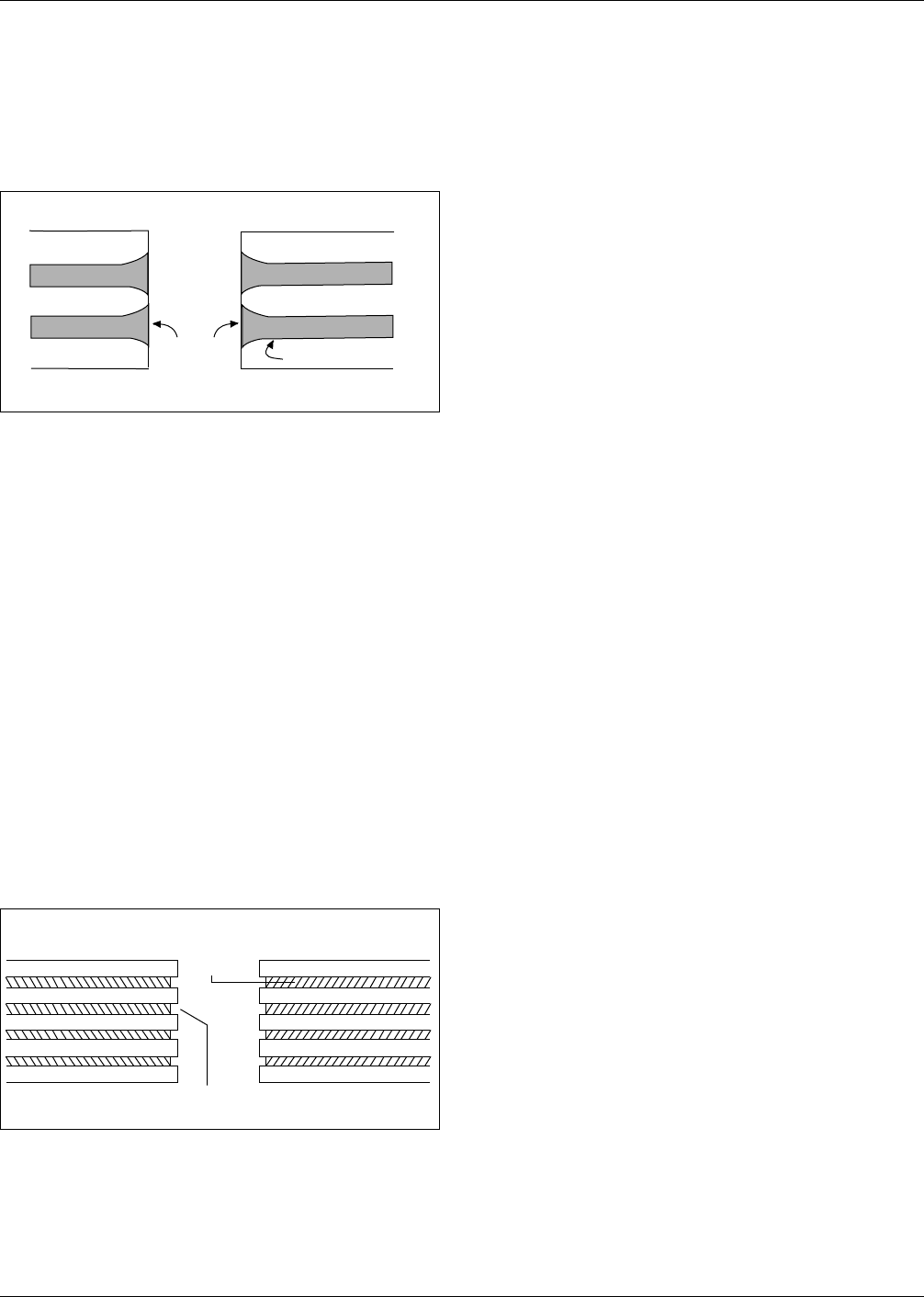
Negative Etchback 54.0798
Etchback in which the inner conductor layer material is
recessed relative to the surrounding base material. (See
Figure N-2.)
Negative (n.) 24.0797
An artwork, artwork master, or production master in which
the pattern being fabricated is transparent to light and the
other areas are opaque.
Negative Pattern 24.1639
An artwork, artwork master, or production master in which
the pattern being fabricated is transparent to light and the
other areas as opaque.
Negative-Acting Resist 52.1448
A resist that is polymerized by light and which, after expo-
sure and development, remains on a surface in those areas
that were under the transparent areas of a production mas-
ter.
Neighborhood Processing 92.0799
The determination of information about a location or pixel
by the use of information obtained about its neighbors.
Nesting 25.1176
Embedding data in levels of other data so that certain rou-
tines may be executed or accessed continuously in loops.
Net 21.1177
An entire string of electrical connections from the first
source point to the last target point, including lands and
vias.
Net List 21.1178
A list of alphanumeric representations, each of which is
used to describe a group of two or more points that are
electrically common.
Nick (n.) 60.1179
A cut or notch in a wire or in the edge of a conductor.
Node 21.1180
The endpoint of an electrical network branch or the junc-
tion of two or more branches.
Nodule 60.1181
A mass or small lump with an irregular shape that is con-
vex to a surface.
Noise (Process Control) 91.1182
Factors in a manufacturing process that are uncontrollable
or too costly to control.
Nominal Cured Thickness 55.1449
The thickness of a multilayer printed board, or the distance
between two two adjacent layers of a multilayer printed
board, after the prepreg has been cured at the temperature
and pressure specified for that particular class of resin flow.
Nominal-Is-Best Characteristic 91.1450
A parameter of quality that optimizes performance at its
nominal value. (See also ‘‘Larger-the-Better Characteris-
tic’’ and ‘‘Smaller-the-Better Characteristic.’’)
IPC-I-001045
Figure N–1 Nail heading
NAIL HEADING
BASE MATERIAL
COPPER CONDUCTOR
LAYER
IPC-I-001032
Figure N–2 Negative etchback
Negative
Etchback
▼
▼
Base Material
Copper
Conductive
Layer
June 1996 IPC-T-50F
45
Nonactivated Flux 75.1183
A natural or synthetic-resin flux without activators.
Nonconductive Pattern 22.1184
A configuration that is formed by the functional noncon-
ductive material of a printed circuit, e.g., dielectric, resist,
etc.
Nonfunctional Interfacial Connection 22.1453
A plated through hole in a double-sided printed board that
electrically connects a printed conductor on one side of the
board to a nonfunctional land on the other side of the
board. (See Figure N-3.)
Nonfunctional Land 22.1185
A land that is not connected electrically to the conductive
pattern on its layer.
Nonfunctional Terminal Area 22.1186
see ‘‘Nonfunctional Land.’’
Nonionic Contaminant 76.1187
A residue that does not readily ionize in water.
Nonpolar Matter 76.1188
A substance that cannot be dissolved in water that is
soluble in hydrophobic solvents.
Nonpolar Solvent 76.1454
A liquid that is not ionized to the extent that it is electri-
cally conductive, that can dissolve nonpolar compounds
(such as hydrocarbons and resins), and cannot dissolve
polar compounds (such as inorganic salts.)
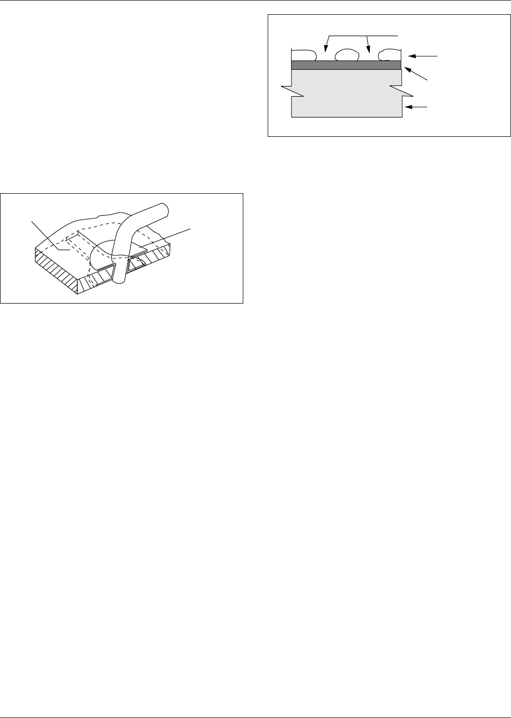
Nonwetting (Solder) 75.1189
The partial adherence of molten solder to a surface that it
has contacted and basis metal remains exposed. (See Fig-
ure N-4.)
Normal Distribution 94.1191
A mathematically-defined continuous distribution of values
that has a bell shape that is perfectly symmetrical about a
mean value.
Normal-Mode Rejection (NMR) 21.1190
The amount of noise superimposed on the input signal of a
direct-current (DC) digital voltmeter that the instrument is
capable of rejecting.
Null Hypothesis 91.1455
The supposition that no significant difference exists
between the desired results of two comparable populations.
(See also ‘‘Alternative Hypothesis’’ and ‘‘Statistical
Hypothesis.’’)
Numerical Control (machine) (NC) 25.1193
The automatic control of electromechanical devices by
means of a digital input to an electronic controller.
Numerical Control (math.) (NC) 20.1192
The use of mathematics to define, design or test geometric
quantities that are used in a computer-aided technology.
O
Object Code 25.0801
The output from a computer compiler or assembler that is,
or is suitable for, processing into executable machine
codes.
Object-Oriented Database 11.0800
A database that combines graphics and text to describe
objects.
Occluded Contaminant 76.0802
A contaminant that is totally contained in an insulating
material.
Occlusion 76.0803
Uniform molecular adhesion between a precipitate and a
soluble substance, or between a gas and a metal.
Off Bond 74.0804
A termination that has some portion of the bonding area
extending off the bonding land.
Offset Land 22.0805
A land that is intentionally not in physical contact with its
associated component hole.
IPC-I-001046
Figure N–3 Nonfunctional interfacial connection
Conductor
Non-
functional
Land
▼
▼
IPC-I-001042
Figure N–4 Nonwetting
NONWETTING
SOLDER
BASIS METAL
BASE MATERIAL
IPC-T-50F June 1996
46