IPC-T-50F_.pdf.pdf - 第53页
Para-aramid 44.1464 The generic term that describes fibers that are made from wholly- aromatic polyamide, amide polymers in which at least 85 % of the amide linkages are directly attached to two benzene rings at the para …
Overcoat 76.0815
A thin film of insulating material that is applied over a
semiconductor die for the purposes of mechanical and con-
tamination protecticon.
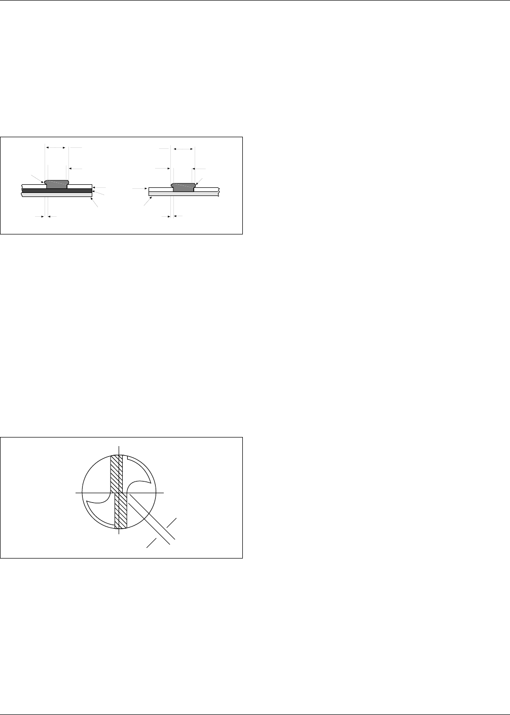
Overhang 60.0816
The sum of outgrowth and undercut. (See Figure O-3.) (If
undercut does not occur, the overhang is the same as the
outgrowth.)
Overheated Solder Connection 75.0817
A solder connection that is characterized by solder surfaces
that are dull, chalky, grainy, and porous or pitted.
Overlap (Film) 67.0818
The contact area between a film component and a film
conductor.
Overlap (Drill) 51.1229
The amount of misalignment between the trailing edge of
the junction line between the primary and secondary drill-
point clearance angles when they are behind the drill cen-
terline. (See Figures B-4 and O-4.) (See also ‘‘Layback.’’)
Overplate 53.1673
Conformal metallic deposition on a previously formed con-
ductive pattern or part thereof.
Oxide Transfer 41.0819
see ‘‘Treatment Transfer.’’
Oxygen Concentration Cell 76.0820
A galvanic cell resulting primarily from differences in oxy-
gen concentration.
P
Package 30.1460
The container for a circuit component, or components, that
is used to protect its contents and to provide terminals for
making connections to the rest of the circuit.
Package Cap 30.0821
A cuplike package cover.
Package Cover 30.0053
The cover that encloses the contents in the cavity of a
package in the final sealing operation.
Package Lid 30.0822
A flat package cover.
Packaging and Interconnecting Assembly 60.0823
The general term for an assembly that has components
mounted on either or both sides of a packaging and inter-
connecting structure.
Packaging and Interconnection Structure 60.1461
The general term for a completely processed combination
of base materials, supporting planes or constraining cores,
and interconnection wiring that are used for the purpose of
mounting and interconnecting components.
Packaging Density 20.1462
The relative quantity of functions (components, intercon-
nection devices, mechanical devices, etc.) per unit volume.
(This is usually expressed by qualitative terms such as
high, medium, and low.)
Pad 20.0824
see ‘‘Land.’’
Panchromatic Emulsion 24.0825
A photographic emulsion that is spectrally sensitive to all
portions of the visible light spectrum.
Panel 41.1463
A rectangular sheet of base material or metal-clad material
of predetermined size that is used for the processing of one
or more printed boards and, when required, one or more
test coupons. (See also ‘‘Blank.’’)
Panel Drawing 26.0826
A document that shows the production master with related
manufacturing patterns and artifacts that relate to the fabri-
cation of printed boards.
Panel Plating 53.0827
The plating of an entire surface of a panel including holes.
IPC-I-001043
Figure O–3 Outgrowth, overhang, and undercut
CONDUCTOR WIDTH
PLATING
CONDUCTOR WIDTH AS ON
PRODUCTION MASTER
BASE MATERIAL
RESIST
METAL FOIL
OUTGROWTH
OUTGROWTH
PLATING
IPC-I-002326
Figure O–4 Overlap
▼
▼
Overlap
IPC-T-50F June 1996
48

Para-aramid 44.1464
The generic term that describes fibers that are made from
wholly- aromatic polyamide, amide polymers in which at
least 85 % of the amide linkages are directly attached to
two benzene rings at the para position in the polymer
chain.
Parallel Pair 22.0828
Two conductors that are side-by-side at a controlled spac-
ing.
Parallel-Gap Soldering 75.1465
The passing of an electrical current through a high-
resistance space between two parallel electrodes in order to
provide the energy required to make a soldered termina-
tion.
Parallel-Gap Welding 75.1466
The passing of an electrical current through a high-
resistance space between two parallel electrodes in order to
provide the energy required to make a welded termination.
Parameter Record 25.0829
A record that defines the characteristics of a subsequent set
of records such as job identification, electrical description,
tolerances, etc.
Pareto Analysis 94.0830
A problem-solving technique whereby all potential prob-
lem areas or sources of variation are ranked according to
their contribution to the end result.
Partial Lift 74.0831
A bonded lead that has been partial removed from the
bonding area.
Partially-Clinched Lead 72.1467
A component lead that is inserted through a hole in a
printed board and is then formed in order to retain the
component in place and but not necessarily in order to
make metal-to-metal contact with a land prior to soldering.
(See also ‘‘Clinched Lead.’’)
Passivation 57.0832
The formation of an insulating layer to protect a surface
from contaminants, moisture and particulate matter.
Passive Base Material 44.0834
Base material, that does not exhibit transistance, that serves
as the physical support and thermal sink for film circuits.
Passive Component (Element) 30.1468
A discrete electronic device whose basic character does not
change while it processes an applied signal. (This includes
components such as resistors, capacitors, and inductors.)
Passive-Active Cell 76.0833
A cell whose electromotive force is due to the potential
difference between a metal in an active state and the same
metal in a passive state.
Paste Flux 75.0836
A flux formulated in the form of a paste to facilitate its
application. (See also ‘‘Solder Paste’’ and ‘‘Solder-Paste
Flux.’’)
Paste, Soldering 75.0835
A soldering method that uses a solder paste applied to the
land, device termination, or both.
Path 20.0837
see ‘‘Conductor.’’
Pattern 20.0838
The configuration of conductive and nonconductive mate-
rials on a base material, and the circuit configuration on
related tools, drawings and masters.
Pattern Area 20.0839
The section of a designated configuration that includes the
pattern and background.
Pattern Plating 53.0840
The selective plating of a conductive pattern.
Peel Strength 92.0841
The force per unit width that is required to peel a conduc-
tor foil from a laminate perpendicular to the surface of the
substrate.
Percent Contribution 91.0842
The amount that a single factor contributes to a total varia-
tion, expressed as a percent.
Percent of the Field of View 92.0843
The specific part of interest of the minimum required field
of view of a magnification device.
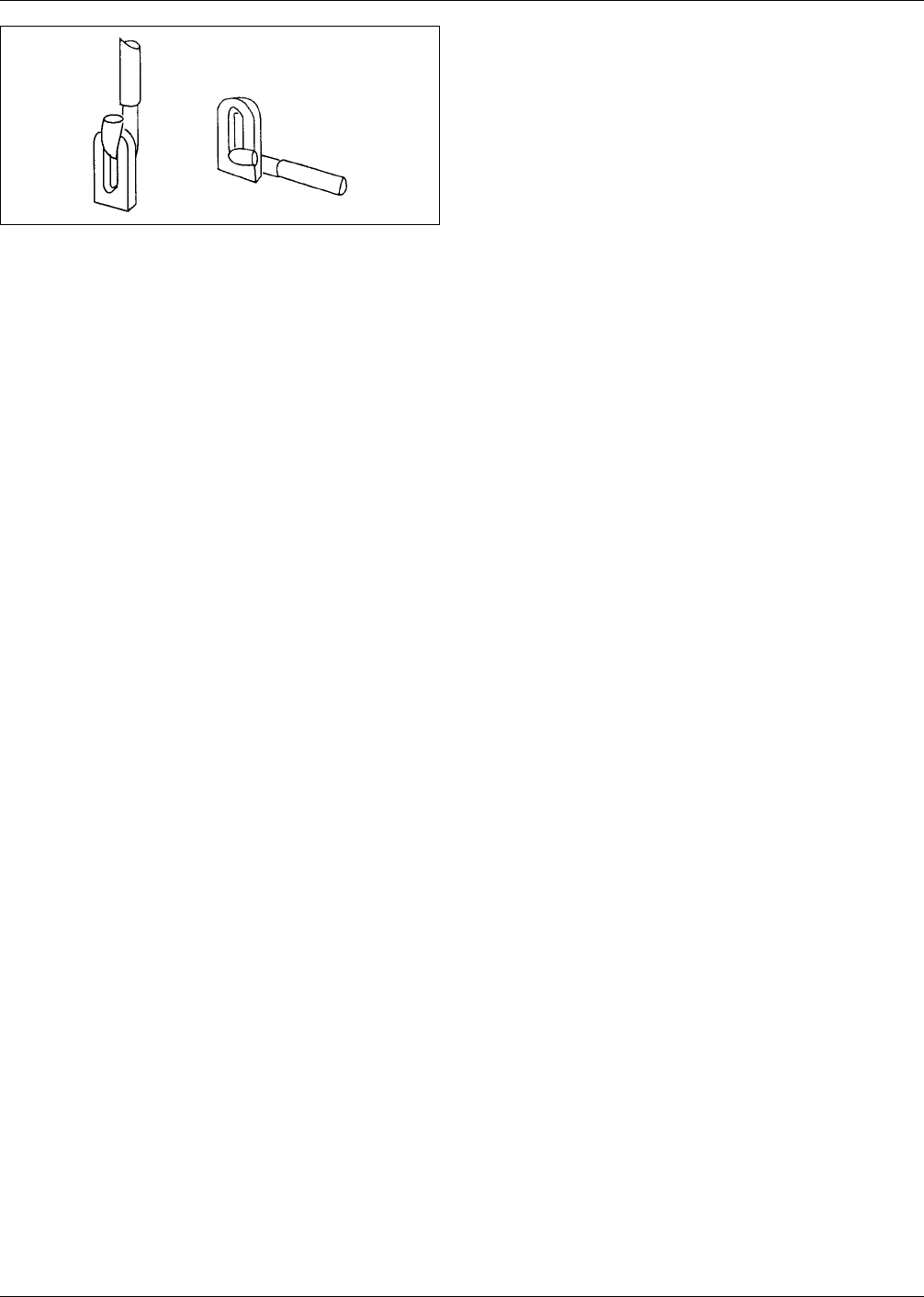
Perforated (Pierced) Solder Terminal 37.1469
A flat-metal solder terminal with an opening through which
one or more wires are placed prior to soldering. (See Fig-
ure P-1.)
Perimeter Sealing Area 30.0844
The surface on the perimeter of the cavity of a package that
is used for attachment to the package cover.
Permanent Resist 52.0845
A resist that is not removed after processing, e.g., plating
resist that is used in a fully-additive process.
June 1996 IPC-T-50F
49
Permeability 21.1803
A general term used to express various relationships
between magnetic induction and magnetizing force.
Permittivity 21.0846
see ‘‘Dielectric Constant.’’
Personality Plate 92.0234
A translator fixture plate drilled to match the product under
test.
Photographic Fog 24.1470
Any unwanted increase in density on a negative-working
photographic product or a loss of density on a positive-
working product that appears on exposed and processed
glass film or paper that is not the result of image exposure.
Photographic Image 24.0456
An image in a photomask or in an emulsion that is on a
film or plate.
Photographic Layer 52.0850
A light-sensitive layer of material that is capable of being
exposed and processed so that it yields a visible image.
Photographic Operation 24.0851
A procedure or technique that prepares a phototool for sub-
sequent processing.
Photographic Plate 24.0852
A ‘‘soda-lime-silica’’ sheet of glass with a photographic
layer.
Photographic-Reduction Dimension 53.0255
The dimensions on an artwork master, such as the distance
between lines or between two specified points, tha indicate
the extent to which the artwork master is to be photo-
graphically reduced. (The value of the dimension refers to
the 1-to-1 scale and must be specified.)
Photomaster 24.0853
see ‘‘Artwork Master.’’
Photometry 24.0854
The measurement of the effect of the intensity and energy
of visible light on the human eye.
Photoplotting 24.0855
A photographic process whereby an image is generated by
a controlled- light beam that directly exposes a light-
sensitive material.
Photoprint 52.0856
The process of forming a circuit pattern image by harden-
ing a photosensitive polymeric material by passing light
through a photographic film.
Photoresist 52.1472
A material that is sensitive to portions of the light spectrum
and that, when properly exposed can mask portions of a
base metal with a high degree of integrity.
Photoresist Image 52.0857
An exposed and developed image in a coating on a base
material.
Phototool 24.0858
A photographic product that is used to produce a pattern on
a material. (see also ‘‘Artwork,’’ ‘‘Artwork Master,’’ ‘‘Pro-
duction Master,’’ ‘‘Working Master.’’)
Phototooling 24.0859
The entire group of photographic products that are used to
produce an pattern on a base material.
Phototooling Aid 24.0860
A photographic product that is used to assist in the inspec-
tion of, but not the transfer of, imaged patterns.
Pick 44.0861
Filling yarn that runs crosswise to the entire width of a
fabric.
Pick-Up Force 73.1760
The force required to pick up a surface mounting compo-
nent from its packaging medium for placement on a sub-
strate.
Pick-Up Tool 73.1759
A tool used to pick up surface mount components from a
packaging medium for placement on a substrate and which
may be hand activated or a part of a pick-and-place
machine.
Pilot Hole 22.0862
see ‘‘Tooling Hole.’’
Pinhole (Material) 92.0863
An imperfection in the form of a small hole that penetrates
entirely through a layer of material. (See also ‘‘Pit’’ and
‘‘Solder Connection Pinhole.’’)
IPC-I-001024
Figure P–1 Perforated (pierced) solder terminal
IPC-T-50F June 1996
50