IPC-T-50F_.pdf.pdf - 第48页
Mounting Hole 20.0779 A hole that is used for the mechanical support of a printed board or for the mechanical attachment of components to a printed board. Muffle 75.0780 An enclosure that is located between the heating e…

Microcomponents 30.0758
Small discrete components.
Microelectronics 30.0759
The area of electronic technology with, or applied to, the
realization of electronic systems from extremely-small
electronic elements, devices or parts.
Microprobe 92.0760
A small sharp-pointed object with a positional handle that
is used to make temporary electrical contact to a land on a
semiconductor for testing purposes.
Microsectioning 92.1447
The preparation of a specimen of a material, or materials,
that is to be used in a metallographic examination. (This
usually consists of cutting out a cross-section, followed by
encapsulation, polishing, etching, staining, etc.)
Microstrip 21.0761
A transmission-line configuration that consists of a conduc-
tor that is positioned over, and parallel to, a ground plane
with a dielectric between them.
Microwave Integrated Circuit 21.0762
An integrated circuit that performs at microwave frequen-
cies.
Migration Rate 96.0763
The distance over which metal migration proceeds in a
given unit of time.
Migration Velocity 96.0764
see ‘‘Migration Rate.
Minimum Annular Ring 22.0766
see ‘‘Minimum Annular Width.’’
Minimum Annular Width 22.0765
The minimum width of metal(s) at the narrowest point
between the edge of a hole and the outer edge of a circum-
scribing land. (This determination is made to the drilled
hole on internal layers of multilayer printed boards and to
the edge of the plating on external layers of multilayer and
double-sided printed board.)
Minimum Electrical Spacing 21.1451
The minimum allowable distance between adjacent con-
ductors, at a given voltage and altitude, that is sufficient to
prevent dielectric breakdown, corona, or both, from occur-
ing between the conductors.
Minor Defect 91.0767
A defect that is not likely to result in a failure of a unit or
product or that does not materially reduce its usability for
its intendeded purpose.
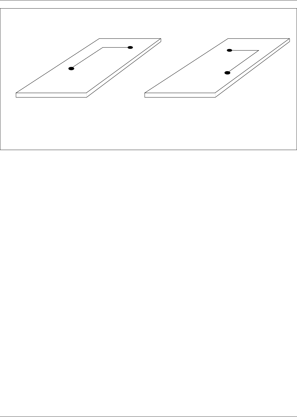
Mirrored Pattern 24.0768
A pattern whose orientation denotes a transposition from
right reading. (See Figure M-2.)
Mis-Pick 44.0769
A break in the pattern of cloth from selvage to selvage that
is caused by a missing filling yarn.
Mislocated Bond 74.0770
see ‘‘Off Bond.’’
Misregistration 50.0771
Imperfect registration.
Mixed Component-Mounting Technology 70.1452
A component mounting technology that uses both through-
hole and surface- mounting technologies on the same pack-
aging and interconneting structure.
Mixed-Effects Model 91.0772
An experimental treatment that contains elements of both
fixed-effects and random-effects models.
Mixed Technology 70.1757
In surface mounting, refers to mixing through hole compo-
nent and surface mounting components on the same side of
a printed circuit board.
Modal Form 25.0773
The technique whereby a data description or other pertinent
command is given only once at the beginning of a related
set of data.
Modification 77.0774
The revision of the functional capability of a product in
order to satisfy new acceptance criteria.
Module 80.0775
A separable unit in a packaging scheme.
Molecular Dye-Imaging Material 24.0776
see ‘‘Diazo Material’’
Monolithic Integrated Circuit 30.0777
An integrated circuit in the form of a monolithic structure.
Montreal Protocol 76.1758
An agreement by industrialized nations, at a meeting held
in Montreal, Canada, to eliminate chlorofluorocarbons
from all processes by 1995.
Mother Board 85.0778
A printed board assembly that is used for interconnecting
arrays of plug-in electronic modules. (See also ‘‘Back-
plane.’’)
June 1996 IPC-T-50F
43
Mounting Hole 20.0779
A hole that is used for the mechanical support of a printed
board or for the mechanical attachment of components to a
printed board.
Muffle 75.0780
An enclosure that is located between the heating elements
and the parts being processed that contains the atmosphere
required for the reflow soldering process.
Multi-Vari 91.0781
A nonmathematical method for determining the sources of
variation.
Multichip Integrated Circuit 86.0782
see ‘‘Multichip Module.’’
Multichip Microcircuit 86.0783
see ‘‘Multichip Module.’’
Multichip Module (MCM) 86.0784
A microcircuit module consisting primarily of closely-
spaced unpackaged semiconductor dice or chip scale pack-
ages, that have a silicon area density of usually more than
of the module area.
Multilayer Carrier Tape 36.0785
Carrier tape with two or more conductor layers.
Multilayer Printed Board 60.1227
The general term for a printed board that consist of rigid or
flexible insulation materials and three or more alternate
printed wiring and/or printed circuit layers that have been
bonded together and electrically interconnected.
Multilayer Printed Circuit Board 60.0786
A multilayer printed board with two or more printed circuit
layers.
Multilayer Printed Circuit Board Assembly 80.0787
An assembly that uses a multilayer printed circuit board for
component mounting and interconnecting purposes.
Multilayer Printed Wiring Board 60.0788
A multilayer printed board with only printed wiring for its
conductive layers.
Multilayer Printed Wiring Board Assembly 80.0789
An assembly that uses a multilayer printed wiring board for
component mounting and interconnecting purposes.
Multilevel Experiment 91.0790
The evaluation of a small number of factors at a large
number of levels.
Multiple Image Production Master 24.1643
A production master having at least two1:1scale patterns
Multiple Indications 91.0791
An anomaly that is detected and reported more than once.
Multiple Pattern 24.1645
The arrangement of two or more1:1scale patterns con-
tained within the size of one panel.
Multiple Printed Panel 50.1646
A printed panel in which one of more patterns occur two
or more times, processed as a single unit and subsequently
divided.
IPC-I-001207
Figure M–2 Mirrored and right-reading patterns
1 2 3 4
Primary Side Viewing
Right Reading Pattern Mirrored Pattern
NOTE: Phototooling emulsion for the right reading pattern is by definition the same as for the
mirrored pattern. That is, both are either emulsion up or both emulsion down.
1 2 3 4
Primary Side Viewing
IPC-T-50F June 1996
44
N
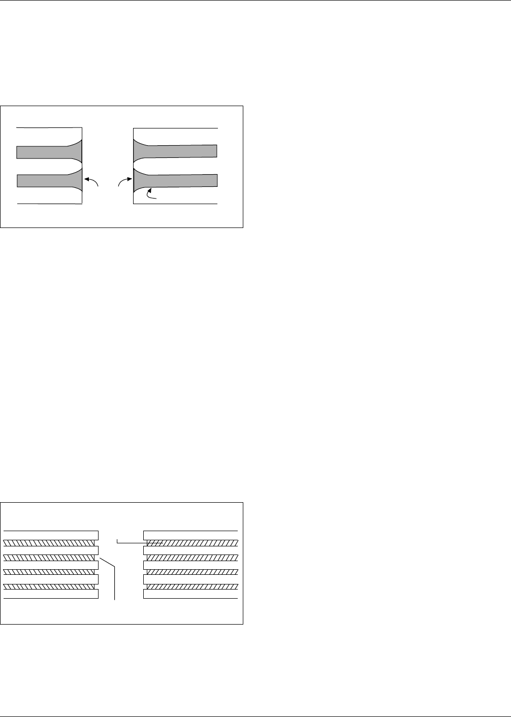
Nail Heading 51.0794
The flared condition of copper on an inner conductive layer
of a multilayer printed board that is caused by hole-drilling.
(See Figure N-1.)
Nail 92.0792
see ‘‘Probe, Test.’’
Nailhead Bond 74.0793
see ‘‘Ball Bond.’’
Near-End Crosstalk 21.0795
see ‘‘Backward Crosstalk.’’
Neckbread 74.0796
A break in a bond immediately above a ball bond.
Negative Etchback 54.0798
Etchback in which the inner conductor layer material is
recessed relative to the surrounding base material. (See
Figure N-2.)
Negative (n.) 24.0797
An artwork, artwork master, or production master in which
the pattern being fabricated is transparent to light and the
other areas are opaque.
Negative Pattern 24.1639
An artwork, artwork master, or production master in which
the pattern being fabricated is transparent to light and the
other areas as opaque.
Negative-Acting Resist 52.1448
A resist that is polymerized by light and which, after expo-
sure and development, remains on a surface in those areas
that were under the transparent areas of a production mas-
ter.
Neighborhood Processing 92.0799
The determination of information about a location or pixel
by the use of information obtained about its neighbors.
Nesting 25.1176
Embedding data in levels of other data so that certain rou-
tines may be executed or accessed continuously in loops.
Net 21.1177
An entire string of electrical connections from the first
source point to the last target point, including lands and
vias.
Net List 21.1178
A list of alphanumeric representations, each of which is
used to describe a group of two or more points that are
electrically common.
Nick (n.) 60.1179
A cut or notch in a wire or in the edge of a conductor.
Node 21.1180
The endpoint of an electrical network branch or the junc-
tion of two or more branches.
Nodule 60.1181
A mass or small lump with an irregular shape that is con-
vex to a surface.
Noise (Process Control) 91.1182
Factors in a manufacturing process that are uncontrollable
or too costly to control.
Nominal Cured Thickness 55.1449
The thickness of a multilayer printed board, or the distance
between two two adjacent layers of a multilayer printed
board, after the prepreg has been cured at the temperature
and pressure specified for that particular class of resin flow.
Nominal-Is-Best Characteristic 91.1450
A parameter of quality that optimizes performance at its
nominal value. (See also ‘‘Larger-the-Better Characteris-
tic’’ and ‘‘Smaller-the-Better Characteristic.’’)
IPC-I-001045
Figure N–1 Nail heading
NAIL HEADING
BASE MATERIAL
COPPER CONDUCTOR
LAYER
IPC-I-001032
Figure N–2 Negative etchback
Negative
Etchback
▼
▼
Base Material
Copper
Conductive
Layer
June 1996 IPC-T-50F
45