DECAN_S2_Admin(Eng_Ver4.5).pdf - 第128页
6-15 Board Definition T each the origin of the small PCB 1. When t he “Enter” key is pressed after teaching, the following screen is displ ayed. T each the origin of the small PCB on the p osition that can determine the …
6-14
Advanced Chip Shooter DECAN S2 Administrator’s Guide
reduce the time.
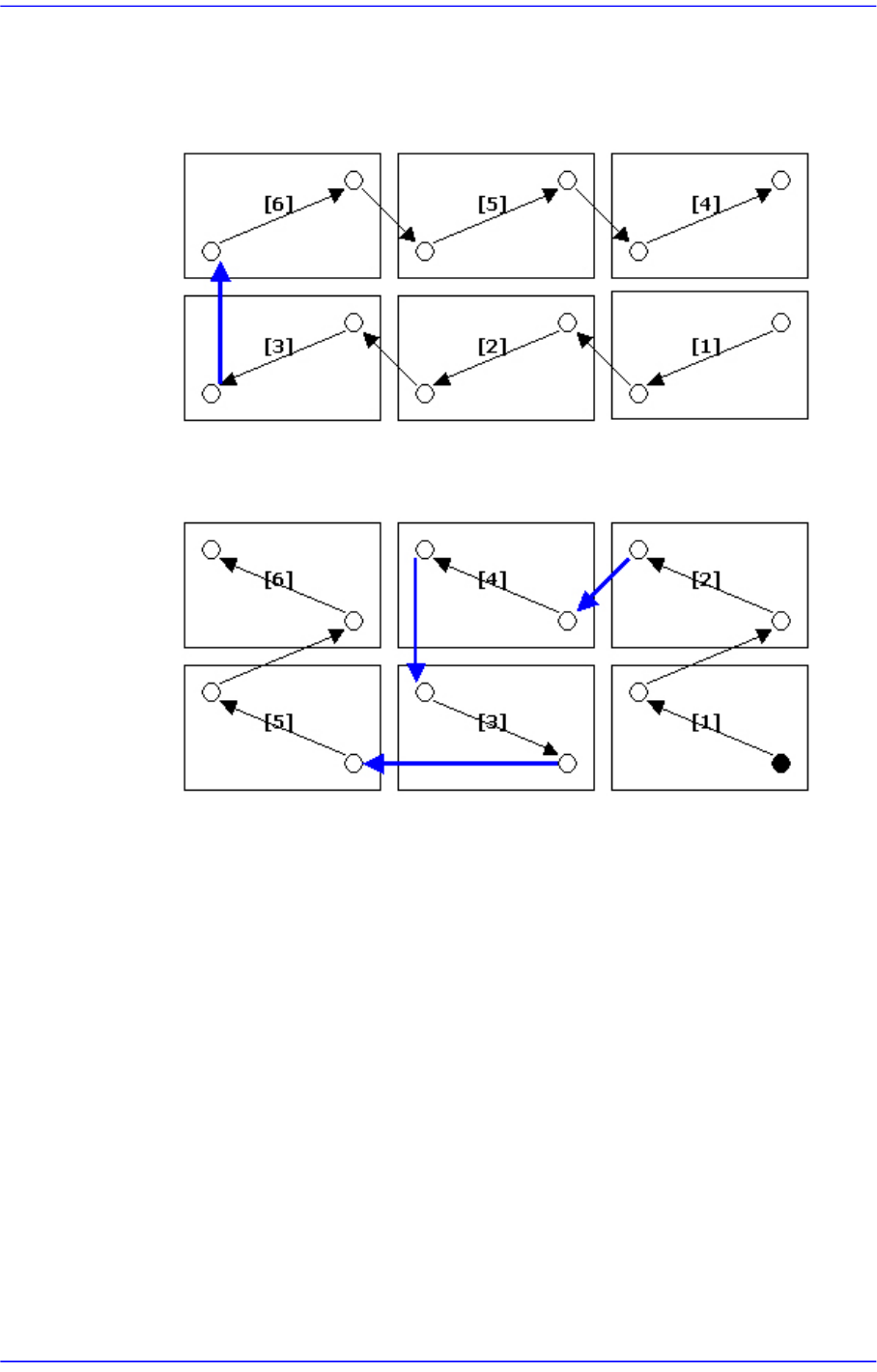
[The order of fiducial teaching when the count direction is selected to X]
1 2 3 6 5 4
[The order of fiducial teaching when the count direction is selected to Y]
1 2 4 3 5 6
<Offset> edit box group
This value is used to set the offset value of the origin of Array PCB automatically.
It sets the placement origin of small PCBs in the array PCB by increasing the
coordinate as much as the offset from the placement origin of the small PCB,
which becomes the reference in the array PCB.
<Teach> button
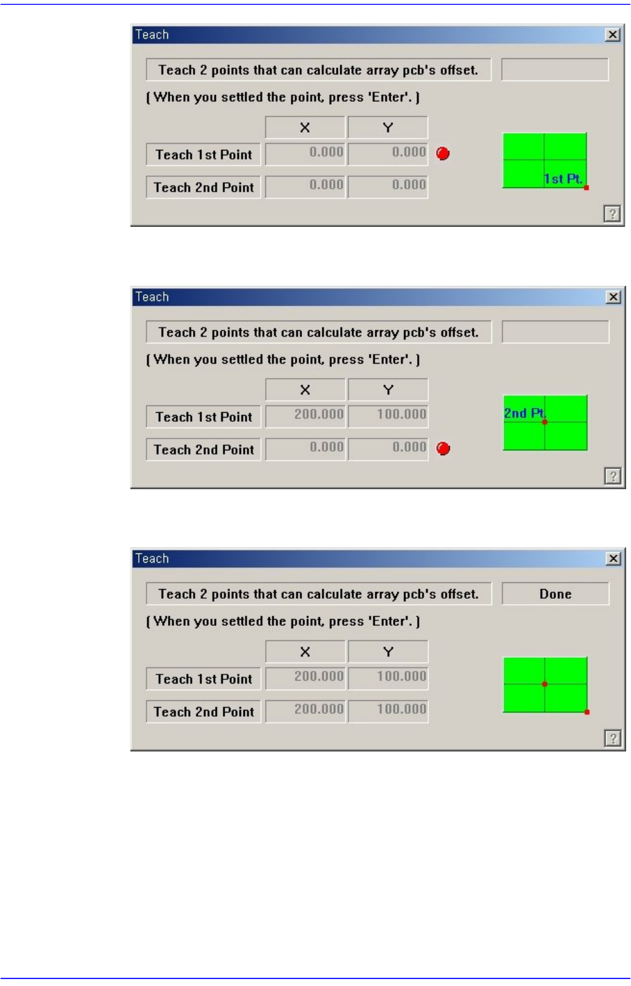
Teach the offset value of Array PCB. When this button is clicked on, the following
screens are displayed in succession.
6-15
Board Definition
Teach the origin of the small PCB 1. When the “Enter” key is pressed after
teaching, the following screen is displayed.
Teach the origin of the small PCB on the position that can determine the offset.
When the “Enter” key is pressed after teaching, the following screen is displayed.
Press the “Enter” key to complete the Array PCB offset value teaching operation.
<Apply> button
Automatically creates Array PCB data with the value set in this group.
<5. Add Value> group
Set the values of X, Y, and R to be added to the grid line of the <1. Array> group.
When the “Add” button is clicked on after setting the desired values, the values are
added to the corresponding grid lines.
6-16
Advanced Chip Shooter DECAN S2 Administrator’s Guide
<Array Skip/Work Tools> group
All Skip: Set “Skip” for all of the array PCBs.
All Work (No Skip): Release ‘Skip’ settings for all of the array PCBs.
Skip: Set the ‘Skip’ for the array PCB having the number that is inputted in the
‘Array No’.
Work Release ‘Skip’ setting for the array PCB having the number that is inputted
in the ‘Array No’.
<Update> button
Saves the edited data and closes the screen.
<Cancel> button
Closes without saving the edited data.
6.3. Fiducial Mark Setup
If there is a fiducial mark on the PCB, set the position of the fiducial mark and mark data.
The fiducial mark is the mark on the PCB used for recognition of the PCB distortion and
its correction. In the case of the PCB without fiducial mark, the placement accuracy is
relatively low.
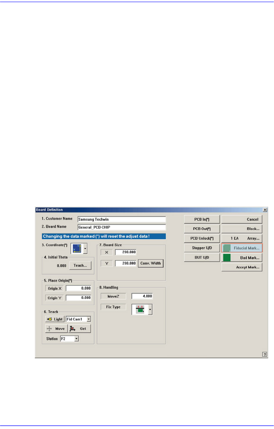
When this <Fiducial Mark…> button is clicked on, the following dialog box is displayed.