M20_Ope_E.pdf - 第156页
Chapter 5 Libraries 5-6 z Applicable Maximum Component Size Camera type Vision process M10/M20 Multi-Scan Camera Whole View 0402 to 40 mm sq. 2 Views Horizontal 80 × 40 mm 2 Views Vertical 40 × 80 mm 3 Views Horizontal 1…
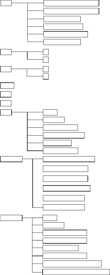
Chapter 5 Libraries
5-5
SOP
X
Y
SOJ X
Y
Connector One-side Leaded (bottom)
One-side Leaded (left)
One-side Leaded (top)
One-side Leaded (right)
Two-side Leaded (X)
Two-side Leaded (Y)
LCC
PLCC
QFP
BGA Matrix
Staggered
Perimeter-matrix
Perimeter-staggered
Partial-matrix
Partial-staggered
BGA/CSP Matrix
Staggered
XY Dif Pitch Matrix
XY Dif Pitch Staggered
White BGA Matrix
White BGA Staggered
White BGA XY Dif Pitch Matrix
White BGA XY Dif Pitch Staggered
CPL
CPL process (top & bottom)
CPL process (right & left)
CPL process (top)
CPL process (right)
CPL process (bottom)
CPL process (left)
Image Processing Area
The image processing area forms a square with a side of double length of a component. If the
area exceeds the FOV of the camera, the FOV is taken as the area.
Camera types to recognize the components
・ Multi-Scan Camera
Chapter 5 Libraries
5-6
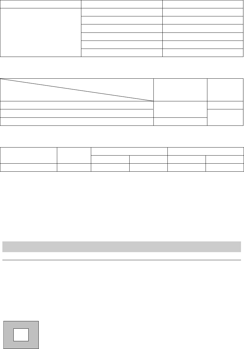
z Applicable Maximum Component Size
Camera type Vision process M10/M20
Multi-Scan Camera Whole View 0402 to 40 mm sq.
2 Views Horizontal 80 × 40 mm
2 Views Vertical 40 × 80 mm
3 Views Horizontal 120 × 40 mm
3 Views Vertical 40 × 120 mm
4 Views 80 mm sq.
Relationship between applicable maximum component size and component height
Component height + PCB thickness
+ pre-mounted component height
Component height
0 to 28 mm 28 to 55 mm
0 to 15 mm
80 m sq./120 x 40 mm
(40 x 120 mm)
36.7 mm sq.
15 to 17 mm
25.4 mm sq.
17 to 25 mm 25.4 mm sq.
z Applicable Minimum Lead Pith/Applicable Minimum Ball Size
Camera type Lead pitch
With ball damage check Without ball damage check
Ball diameter
Ball pitch Ball diameter Ball pitch
Multi-Scan Camera 0.3 mm 0.2 mm 0.4 mm 0.4 mm 0.65 mm
Vision Processing Algorithm for each Component type
The following section shows the application of components and cameras for each vision
process method. However, the available component size below can be limited by actual
Camera specification on the machine.
(Refer to the “Details of Vision Processing Modes” on following pages for details.)
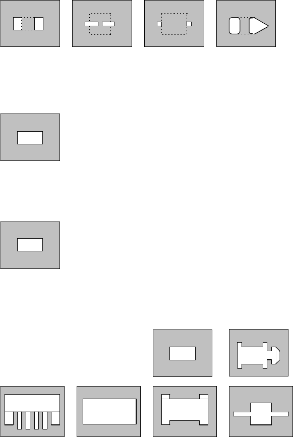
Chips
Chip
Note: For the component which has difficulty to be processed by standard mode, try with other
modes for special component. Finally select the best mode for the component.
● CPL Process Rectangular. Overall parts reflect light: (for standard
chip-type components)
Multi-scan camera Chip size: 0402 or larger
Chapter 5 Libraries
5-7
● Electrolytic Capacitor Two terminations reflect light: ( for standard two
leads component such as electrolytic capacitor)
Multi-scan camera Termination size: 0.5 mm sq. or larger
● Edge-midpoint search Chips. Overall parts reflect light: (for special type
(Fastest process) component)
Multi-scan camera Chip size: 0402 or larger
● Corner search Chips. Overall parts reflect light: (for special type
component)
Multi-scan camera Chip size: 0.5 mm sq. or larger
● Overall Chip Process Rectangular. Overall parts reflect light: (for special
type component)
Multi-scan camera Chip size: 1.25 mm sq. or larger
● Glass Melf Cylindrical-shape-glass-encapsulated
Two electrodes reflect light.
Multi-scan camera Outside diameter: 1.0 mm or larger