DECAN_S1_Administrator′s_Guide(Eng_Ver1.5)_Print.pdf - 第142页
6-28 Next Generation, Multi-Functional Plac er DECAN S1 Administrator’s Guide Memo Even though fiducial mark teaching is performed by changing the workstation, all placement coordinates, fiducial mark coordinates a nd th…
6-27
Board Definition
Perform tuning at least more than twice.
9) Reflect set value: Click the <Update> button
6.3.2. Definition of fiducial mark
The method to define the fiducial mark size for a PCB length is as follows:
Length less than 800 mm: Same as the method to set general boards.
Length is 800 mm ~ 1,500 mm: Set multi work area.
6.3.2.1. Fiducial mark setup
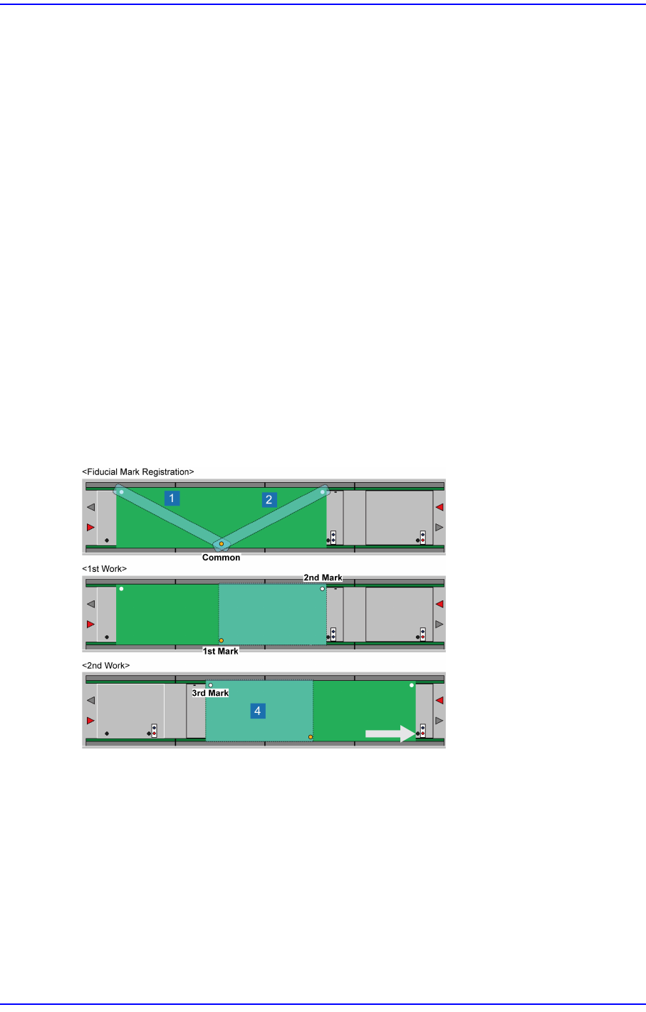
When placing parts on a 0.8~1.2 m long PCB, set 3~4 fiducial marks on it, one of which
must be at the position to which the fiducial camera of the gantry can move.
When setting 3 fiducial marks, they can be set as shown in the following figure.
1) Transfer the PCB to the first workstation.
2) Teach the fiducial mark at center and the right mark.
3) Transfer the PCB to the second workstation.
4) Teach the left fiducial mark.
1: Fiducial mark for ST-Gate2
2: Fiducial mark for ST2F-Work
3: Placement point registered to the ST2F-Work
4: Placement Point registered to the ST-Gate2
6-28
Next Generation, Multi-Functional Placer DECAN S1 Administrator’s Guide
Memo Even though fiducial mark teaching is performed by changing the
workstation, all placement coordinates, fiducial mark coordinates and
the coordinates of various marks are always constant because the
relative distance from the origin is taught.
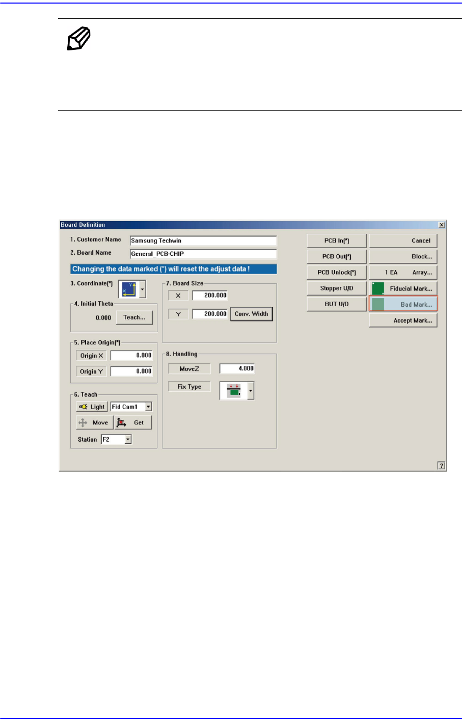
6.4. Bad Mark Setup
The ‘Bad Mark’ refers to the mark indicated on the PCB to show whether a small PCB in
the array PCB is good or defective. Placement is not performed on the small PCB
indicated defective.
When this <Bad Mark…> button is clicked on, the following dialog box to edit bad mark
data is displayed.
6-29
Board Definition
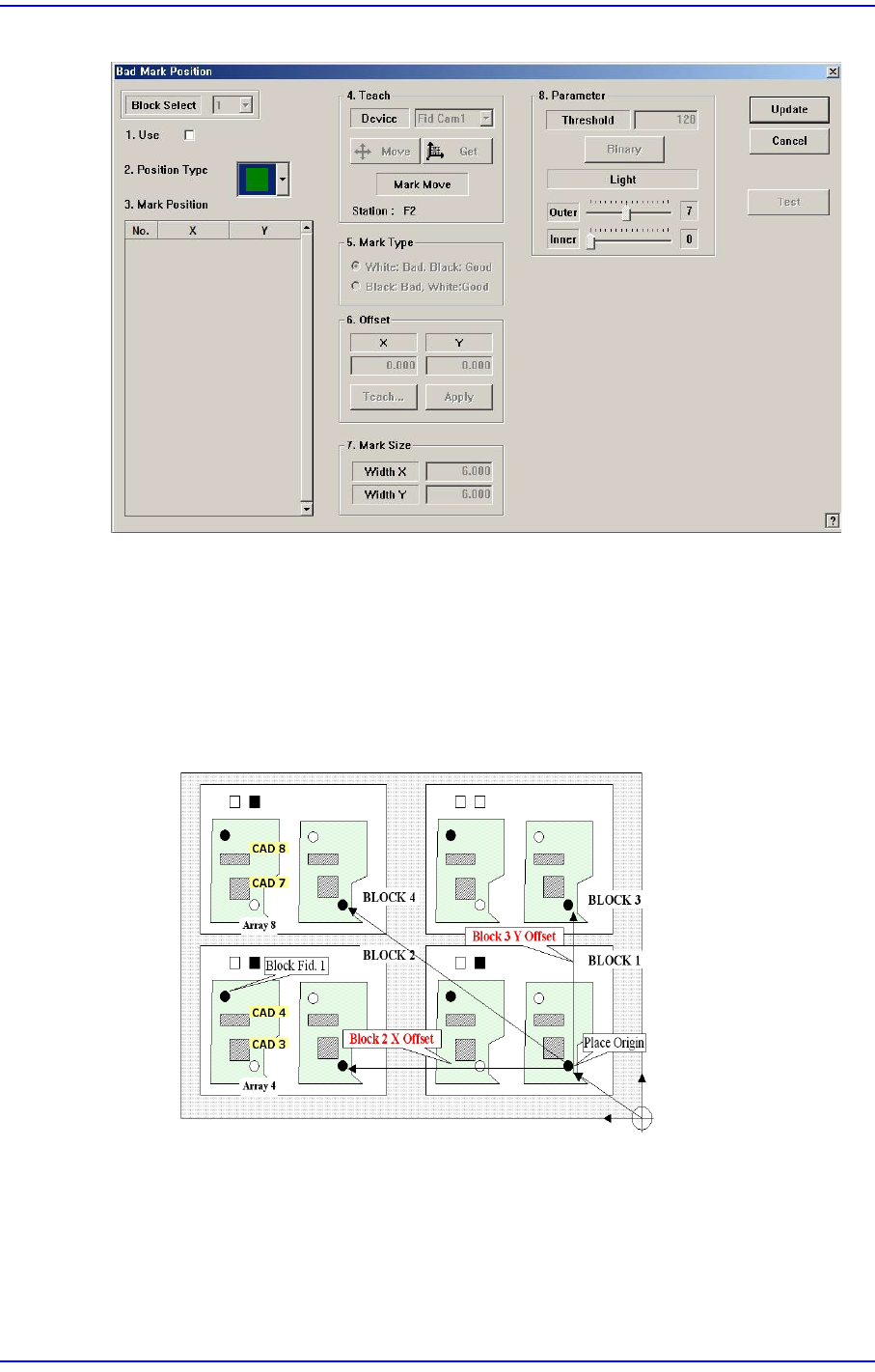
Figure6.6 “Bad Mark Position” dialog box (When the Position Type is “None”)
<Block Select> combo box
For a Multi PCB
The model selected from the “Board Definition” dialog box is selected
automatically and the corresponding combo box is disabled..
For a Block PCB
Select the model for which setup will be performed and set other items.
<1.Use> check box
Determines whether to use a bad mark.
<2. Position Type> combo box
Select a bad mark type. The bad marks that can be selected are as follow;