IPC-D-279 EN.pdf - 第106页
changing the materials of joint height, adding compli- ant leads, or changing the materials of substrate or component to decrease the ∆α . • Perform DfM review of printed board layout- include ease of inspection and rewo…

specifications (PTV T/S, Solder Resistance, IPC-SM-
840, etc.) should be defined with agreed upon test
methods for evaluation.
F-12.2 Printed Board Conductor Design
• Only as needed, use minimum spacings from conduc-
tors to (conductor, mounting hole, component termi-
nals) and from barrels to inner plane conductors and
other barrels
• Minimize electromigration stresses by minimizing
temperature and current density/current crowding:
• Use conductor widths adequate to limit ∆T
conductor
less
than 5°C.
• Use rounded corners
• Use minimum number of sharp/acute angles
• Use smooth transition fillets
• (With the above techniques, conductor cracking, foil
lifting, voltage breakdown are also improved)
• Use metal deposition techniques which result in large,
ductile grains
• Selectively plate pressure contact areas for reliable
electrical contact to avoid ‘‘fretting’’ corrosion; e.g.
gold to gold or tin to tin but not gold to tin. Gold
which is pore-free and ~0.6 µm is required for pressure
connections capable of ‘‘many’’ disconnects and for
SM boards, may require selective gold plating. A
nickel underplate of ~2 µm is required to prevent dif-
fusion of copper into the gold.
• Subdivide large copper areas on the surface to prevent
blistering/solder thieving
• Widen conductors which function as heat dissipators
F-12.3 Solder Joints
See section 4.6 and Appendix A for details.
Identify risk sites for solder joint non-reliability factors
such as:
• Large ∆α between component and substrate, particu-
larly for ceramic components on FR-4 substrate or
plastic components on ceramic substrate.
• Large components on any edge
• Non-compliant leads (short and stubby)
• Large ∆T in the use environment under power cycling
conditions
• Thin solder joints
• Solder joints containing gold > 3 weight percent
Gold thickness is more critical in SM than in TH
because the volume of solder is limited to that of the
paste ‘‘brick’’ and the gold content in the final SM
joint is not as dilute as in the TH joint.
Use printed board gold plating finish 0.1 µm on printed
board surfaces to be SM soldered so that gold concen-
tration is < 3 weight percent in the final joint to avoid
significant solder joint embrittlement. See the note
above on gold thickness required to assure reliable
pressure connections.
Dipping of the component leads in molten solder to
dissolve and remove the thick gold is one historical
method of ‘‘converting’’ gold plate part finishes to a
safe termination finish; the resulting ‘‘solder dip’’ fin-
ish thickness is not uniform and may interfere with the
formation of uniform solder joints.
• Solder joints to terminations finishes containing silver
Joints to components can fail immediately if the termi-
nations are manufactured with a final terminal finish of
silver paste or palladium-silver paste; these materials
rapidly leach into molten lead-tin solder and the result-
ing joint is weak. Avoid leaching by requiring a barrier
metal layer of nickel over the silver for SM component
termination. Thin silver or palladium plating over the
nickel barrier is acceptable; the small amounts of Inter-
metallic Compound (IMC) formed are not detrimental.
Alternatives required to allow silver in the manufactur-
ing process and which result in reliable joints are
— expensive in terms of hand labor, special processing
or special materials
— use special silver-bearing solders in production,
rework and field repair
— limit exposure of the solder joint to solder tempera-
ture
— limit volume of lead-tin solder in the joint; this
alternative may result in reducing solder attachment
cyclic fatigue life.
• Solder joints to final terminations finish of nickel.
Nickel metallization as a final termination finish
results in highly variable solderability or poor solder
joint yields if an aggressive flux is not used in SM
reflow. Nickel is rapidly passivated (covered by a hard,
tenacious, non-solderable oxide). In their journal,
Siemens has reported the use of selective nickel plat-
ing on TAB leads to limit the spread of solder. The
consequences of using a nickel termination finish may
be extensive (uncontrolled) hand soldering to obtain
satisfactory metallurgical joints at the cost of degrad-
ing component reliability.
Strikes of porosity-free palladium or gold, on the order
of 0.1-0.2 µm, can preserve the solderability of the
nickel; silver plate on the order of 20-40 µm and tin or
tin-lead on the order of 400-100 µm are also used for
this purpose.
• Estimate solder joint reliability (see Appendix A).
• Solder joint risk reduction techniques include increas-
ing the solder joint height, adding compliant leads, or
IPC-D-279 July 1996
94

changing the materials of joint height, adding compli-
ant leads, or changing the materials of substrate or
component to decrease the ∆α.
• Perform DfM review of printed board layout- include
ease of inspection and rework of all solder joints, par-
ticularly those adjacent to ‘‘tall’’ components such as
connectors or in the PWA ‘‘valley’’ between such com-
ponents. Placing the non-termination portion of the
SMT component next to the TH component eases
inspection. Packages with heatsinks overhanging the
package edge lack inspectability and have a thermal
shadowing effect on neighboring parts during reflow; a
‘‘shadowed’’ part may require removal of the heat-
sinked part for rework.
July 1996 IPC-D-279
95
Appendix G
Coefficient of Thermal Expansion
G-1.0 COEFFICIENT OF THERMAL EXPANSION
Polymer systems expand with increasing temperature, dem-
onstrating a glassy phase response with a coefficient of
thermal expansion (CTE) or α
1
below T
g
, and a rubbery
phase response with a much higher α
2
, typically 3 times α
1
above T
g
. The transition from glassy phase to rubbery
phase is gradual, but for most polymer substrates may be
characterized by T
g
, the glass transition temperature. See
IPC-T-50.
Glass fiber reinforced substrates exhibit significantly differ-
ent CTE in the z (CTE(z), out of plane) axis compared to
the CTE in the x-y axes; for example, below its T
g
, Quartz/
Bismaleimide material with 35% resin by weight exhibits a
CTE(x,y) of 6 ppm/°C and a CTE(z) of 41. Woven glass
fiber reinforcement exhibits an additional difference
between x and y axes on the order of 1-5 ppm/°C; this dif-
ference may be significant where the CTE of a large SM
component package is to be matched to the CTE of the
substrate to enhance cyclic life of the solder attachments.
The CTE(z) is particularly significant in determining the
cyclic life of PTH and vias in SM PWAs because the aspect
ratio (ratio of substrate thickness to finished hole diameter)
is generally much larger than the corresponding aspect
ratio achieved in printed boards manufactured for through
hole technologies. Higher CTE(z) values result in higher
cyclic tensile stress in the barrel of the PTH or via during
temperature excursion during SM reflow, or SM compo-
nent removal/rework/repair as well as during printed board
fabrication, solder dipping, hot air leveling, or wave solder.
See IPC-TR-579 and IPC-SM-782.
The thermal cycle reliability, vibration robustness, and the
thermal management of high performance Surface Mount
(SM) products are heavily dependent upon the constraining
core such as Copper-Molybdenum-Copper (CMC),
Copper-Invar-Copper (CIC) and Molybdenum-Graphite-
Molybdenum (MGM) composite material systems.
The ratios of the various materials in those composite sys-
tems can be adjusted to tailor the effective CTE to the opti-
mum value. The tradeoffs include weight and cost. See
IPC-MC-324.
G-2.0 CONSTRAINING CORES
A constraining core is an internal supporting plane in a
packaging and interconnecting structure, used to alter the
coefficient of thermal expansion of printed boards.
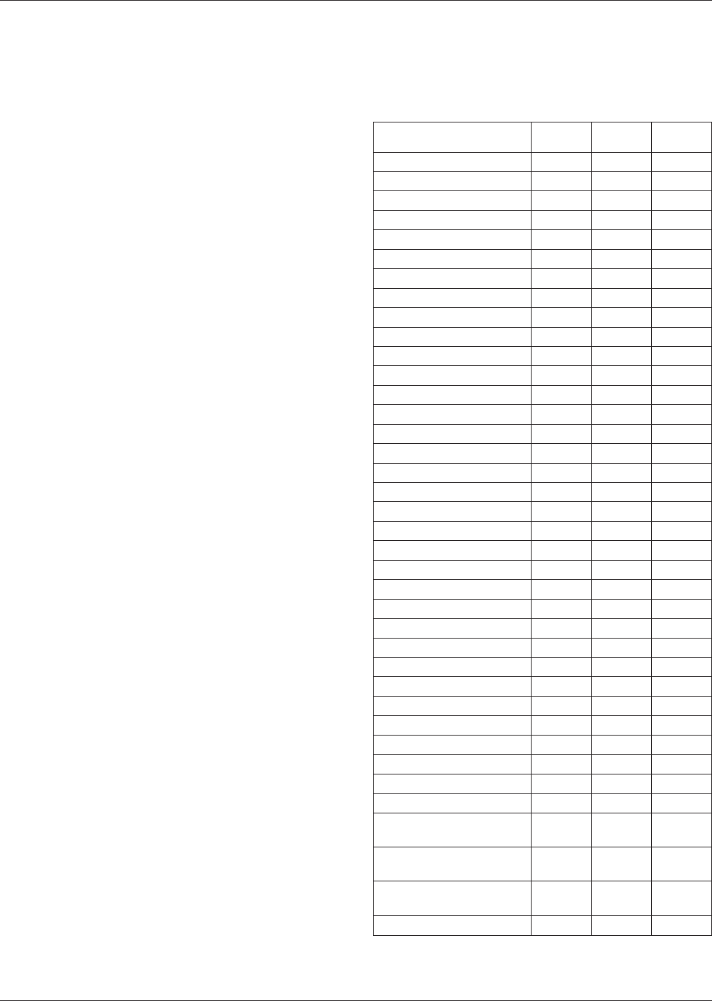
Table G−1 Typical Values for Coefficients of
Thermal Expansion (ppm/°C)
Insulator/Substrate
Material/System
CTE
lower value upper
E glass 5.5
S Glass 2.6
Glass-Ceramic > 3.0
Silicon 2.6
Diamond 0.9
Aluminum Nitride 4.5
Silicon Nitride 3.7
Quartz, fused silica 0.5 0.6
Kevlar 49 -5
Beryllia 6
Cubic Boron Nitride
x-y 3.7
z 7.2
E Glass/Epoxy
x-y 14.2 17.3
x8090
E Glass/Polyimide
x-y 12 16
z6
E Glass/PTFE
x-y 24
z 260
Kevlar/Epoxy
x-y 5.1 7.1
z 5.1 7.1
Kevlar/Polyimide
x-y 3.4 6.7
z83
Quartz/Polyimide
x-y 5.0 8.0
z 68.4
Quartz/Bismaleimide
x-y, 35% Resin 6.2 6.3
z, 35% Resin 41
Alumina (90%) TF
Substrate
7.0
Alumina (Ceramic Chip
Carrier)
5.9 6.5 7.4
Epoxy (70% Silica) Plastic
Packaging
20 23
Mulite Co-Fired 4.2
IPC-D-279 July 1996
96