IPC-D-279 EN.pdf - 第38页
respective land areas is necessary for complete solder joint formation, and thereby contributes to solder joint reliabil- ity . Fully automated pick-and-place equipment requires the use of fiducials (which are designed in…
or;
2. Apply solder paste to side 2, dispense adhesive to
side 2, place SM components, cure/bake adhesive/
paste, invert board, apply solder paste to side 1, place
SM components, reflow solder paste, clean, test/
repair.
With mixed technology boards containing surface mounted
and through-hole components on more than one side of the
substrate (Type 2C - Figure 7-4), there are several typical
sequence possibilities:
1. For SM components on side 2 only: Apply adhesive
to side 2, place SM components, cure adhesive,
clean, invert board, insert through-hole components
and clinch, wave solder, clean test/repair.
or;
2. For SM components on both sides: Apply solder
paste to side 1, place SM components, reflow solder
paste, clean, invert board, apply adhesive to side 2,
place SM components, cure adhesive, invert board,
insert through-hole components and clinch, wave sol-
der, clean, test/repair.
3. For SM components on both sides: Apply adhesive to
side 2, place SM components, cure adhesive, apply
solder paste to side 1, place SM components, reflow
solder paste, clean, invert board, insert through-hole
components and clinch, wave solder, clean, test/
repair.
or;
4. For SM components on both sides: Apply solder
paste to side 1, place SM components, reflow solder
paste, clean, insert through-hole components and
clinch, apply adhesive to side 2, place SM compo-
nents, cure adhesive, invert board, wave solder,
clean, test/repair.
7.1 Solder Paste Application Solder paste may be
applied to a substrate either by syringe application or
screen/stencil printing. The first issue impacting reliability
at this stage is the alloy composition of the solder paste
being deposited. Solder comes in a variety of alloys includ-
ing combinations of tin, lead, silver, antimony, bismuth,
indium and cadmium. Each alloy has a distinct set of met-
allurgical properties and the selection should be based on
compatibility with the metals being joined (including
leaching and intermetallic formation), the service environ-
ment and the service/process temperatures. Reliability will
also be affected by the type of flux system used in the sol-
der paste; high reliability applications should be limited to
the use of R (rosin) or halide-free RMA (rosin-mildly acti-
vated) types.
Another contributor to reliability in this assembly operation
is the volume of solder paste deposited since it will dictate
the size of the solder joint. Careful consideration should be
given to parameters that will affect solder volume such as
stencil thickness and aperture sizes, squeegee/syringe pres-
sure, metal content of the solder paste and thickness of sol-
der coating on the printed board or substrate. See Appen-
dix M for details.
7.2 Adhesive Application Adhesive used to mount com-
ponents for subsequent wave soldering is typically applied
via a syringe dispensing method (either manual or auto-
matic). The volume of deposited adhesive should be
adequate to restrain the part in place but not impinge on
land areas or affect solderability and solder joint formation.
All adhesives should be tested for their tendency to form
voids that can entrap flux and affect long term reliability.
Adhesive voids may also be caused by curing the material
too rapidly. Adhesives may outgas even after complete cur-
ing.
7.3 Component Placement The placement of compo-
nents on the substrate may be accomplished either manu-
ally or by using a broad range of pick-and-place equip-
ment. Accurate positioning of components to their
IPC-279-10
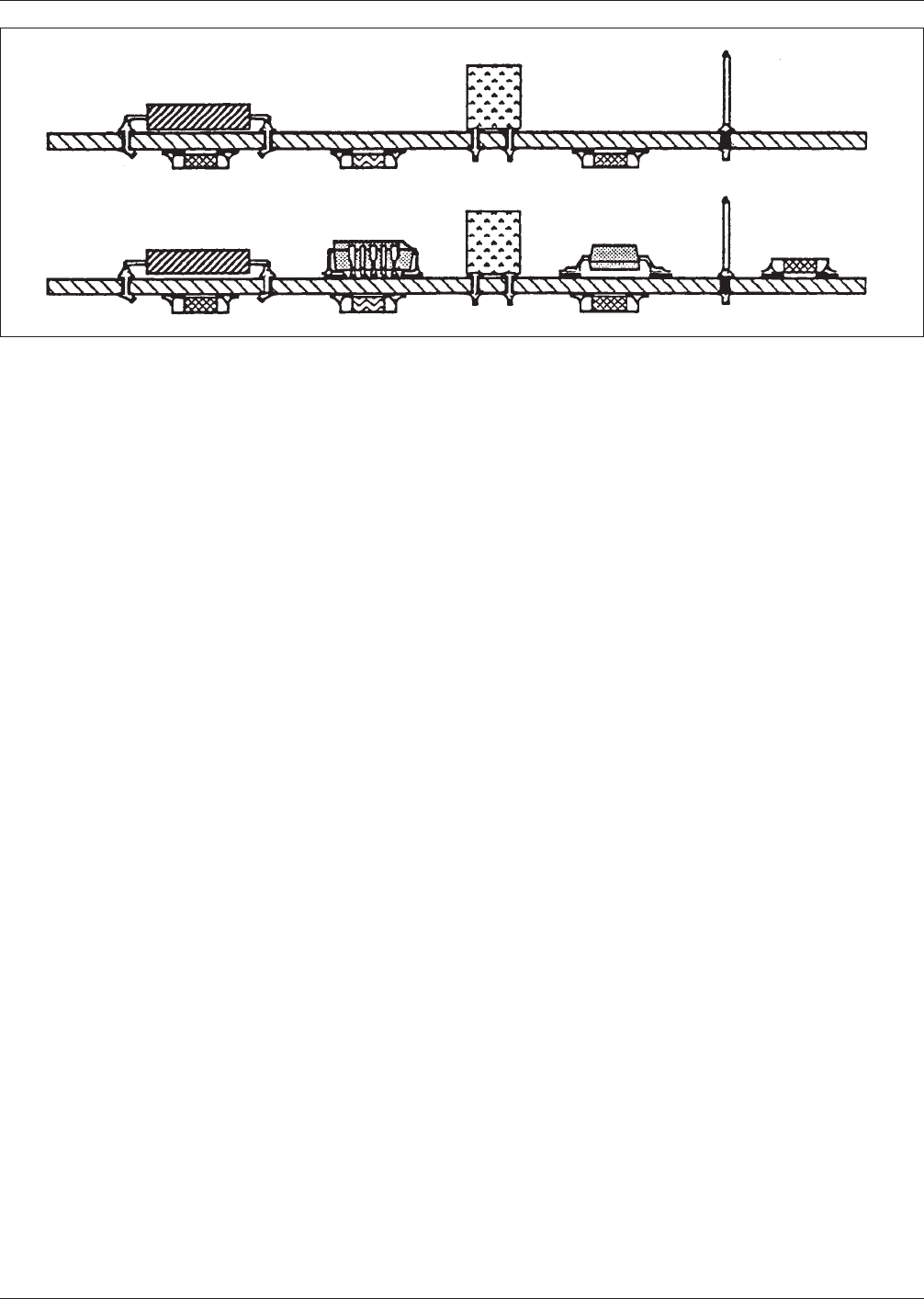
Figure 7−4 Type 2C − Mixed Technology
IPC-D-279 July 1996
26

respective land areas is necessary for complete solder joint
formation, and thereby contributes to solder joint reliabil-
ity. Fully automated pick-and-place equipment requires the
use of fiducials (which are designed into the bare printed
board) for the accurate alignment of the components rela-
tive to the substrate. Fine pitch components often require
their own set of fiducials near or inside the footprint to
assure accurate placement. The type of fiducial (circle,
cross, pound sign, etc.) that works best depends on the par-
ticular assembly equipment used. Refer to IPC-SM-782 for
fiducial and land pattern information.
Bent and skewed component leads may also contribute to
improper location of some leads relative to their corre-
sponding pads, leading to solder wicking and incomplete
solder joints. Checks for lead coplanarity are often done for
high reliability assemblies.
For large volume manufacturing, the placement of smaller
substrates in a panelized format with snap-out features or
scored edges provides more efficient assembly and results
in potentially less handling damage. Care must be taken to
design these features correctly to prevent damage to solder
joints and board interconnects upon separation of the indi-
vidual assemblies from the panel.
7.4 Soldering
7.4.1 Solder Paste Reflow
Solder paste reflow is typi-
cally performed by forced convection, infrared, vapor
phase, or laser soldering process. Important parameters that
will affect the reliability of the components and assembly
include: heating ramp rate, peak temperature in preheat,
time above the minimum reflow temperature (20°C above
liquidus for copper), peak reflow temperature and cooling
rate and duration above the glass transition temperature of
the substrate. Control of the reflow profile is required to
minimize damage to the components and printed board and
to control the formation of intermetallic compounds at the
solder-substrate interface. The formation of appreciable
intermetallic compounds has been identified as one of the
main sources of solder joint failure. See also IPC-SM-816.
High pin count, plastic leaded chip carriers, thin quad flat
packs, thin small outline packages and small outline ICs
(PLCCs, TQFP, TSOP, and SOICs) may exhibit cracking of
the plastic package upon reflow. See 5.3.5 and Appendix
F.6.
7.4.2 Wave Soldering The wave soldering of surface
mount components requires that the parts be correctly ori-
ented during the design phase. If this is not performed, the
terminations may be soldered using specialized wave
geometries (e.g. dual or vibrating wave), however, the trail-
ing terminations will exhibit oversized solder fillets that
may stress and crack chip components.
A good solder joint can form only if the flux has properly
cleaned and prepared the surfaces for the molten solder.
Therefore, activity of the flux is a parameter that needs
close monitoring to prevent dewetted and nonwetted solder
joints. As with reflow soldering, a good soldering profile is
essential to reducing solder defects and preventing thermal
shock cracking of chip capacitors.
The presence of contamination in the solder greatly
impacts the appearance and integrity of the solder joint.
Gold in sufficient quantities (> 3% by weight) can result in
seriously embrittled joints. Solder bath contaminant levels
should be regularly monitored and limited to the levels
found in IPC-S-815.
Active plastic packages such as SOICs and PLCCs may be
adversely affected by wave soldering if flux seeps into the
lead frame. There is a potential for this to happen since the
lead frame and molding compound have different coeffi-
cients of expansion. Passive components may exhibit
leaching of the precious metal terminations during wave
soldering. If dwell time in the solder wave is minimized
(3-4 seconds), leaching on these parts can be prevented by
a nickel barrier underplating between the precious metal
adhesion layer and the solder coating.
7.5 Cleaning Due to the low clearance of many surface
mount components, flux residues become entrapped under-
neath. Remaining flux may eventually cause corrosion and
electrical malfunctioning, hence, complete removal of
active flux residues are essential to long term reliability.
Following soldering, it may be necessary to initiate imme-
diate cleaning to prevent hardening of the flux that makes
removal difficult. The effectiveness of the cleaning process
should be monitored by measuring ionic residues. See the
test procedures in J-STD-001.
Besides flux, it may be necessary to remove a range of
other residues such as solder oils, dross particles, strippable
solder mask materials, solder balls and particulate matter.
The cleaning medium (solvent) can adversely affect the
solder mask, printed board, conformal coating, board or
component legends/marking/labels, thin or mechanically
stressed sections of plastic components. Appendix I dis-
cusses the specifics of solvent compatibility on various
plastics and metals.
7.6 Rework/Repair Repair and rework equipment are
typically one of two types: hot air devices and conductive
tips. When hot air devices are used, care should be taken
to prevent thermal damage to adjacent components and the
surrounding area of the printed board. The number of times
that a part is removed and replaced should be limited in
order to prevent internal thermal damage such as intercon-
nect separations within the substrate. Desoldering time
when using conductive tips should be limited to three sec-
onds to prevent thermal damage. See IPC-R-700 for
rework and repair methods. See 7.8.1.2 for reliability
impacts.
July 1996 IPC-D-279
27

RO-L0, RE-L0, RO-L1 flux per J-STD-004 should be used
during rework operations and the component should be
cleaned immediately following rework. Compatibility of
the flux used in repair/rework with the flux used in the
original processing should be assumed prior to repair/
rework. Only RO-L0 or RE-L0 flux should be used in
repair or rework of conformally coated assemblies as typi-
cally the conformal coating will not withstand exposure to
cleaning processes necessary to completely clean activated
flux (e.g., L1, formerly RMA or RA) flux residues. For
no-clean manufacturing processes, no cleaning should take
place following touchup or repair.
7.7 Depaneling Surface mount assemblies that have
been panelized to facilitate handling during the assembly
steps will eventually need to be removed from the panel for
use. Depaneling may be required before or after electrical
testing (based on the design of the test fixture). Individual
board assemblies are typically attached together by webs of
substrate material that are left following partial routing of
the board outline. These webs may contain drilled holes to
promote easy ‘‘snap-out’’ of the individual boards. Also
common is the use of scoring (either from one or both
sides) which produces a groove to assist with depaneling.
It is also possible to completely rout the boards from the
assembled panel.
The depaneling operation exerts large mechanical stresses
throughout the substrate and assembly. Extreme care must
be taken to limit these stresses so that their impact on the
board interconnects and surface mount solder joints is
minimized.
7.8 Design for Manufacturability
7.8.1 Components
7.8.1.1 Soldering Effects
The design process must con-
sider the effects of soldering on components in order to
produce a reliable assembly.
Components that may be susceptible to degradation from
thermal excursions caused by soldering include plastic film
capacitors, pulse transformers, inductors, delay lines, pas-
sive networks, relays, crystals, and crystal oscillators. In
some instances, insulative or reflecting heat shields may
provide sufficient thermal isolation. Where the thermal
limitations arise from other causes such as internal plastics
with low melting or softening point (e.g., plastic film
capacitors, light emitting diodes (LEDs)), or internal liq-
uids with low boiling point (e.g., liquid electrolytic capaci-
tors or batteries), internal plastics with high CTE, repre-
senting a large fraction of the package volume (e.g., silicon
stress relief coating of pulse transformers, passive delay
lines), or structural materials of low deflection temperature
thermoplastic materials (e.g., connectors or sockets), the
same general alternatives apply.
Where there are thermally massive components such as
high pin count connectors, sockets, PGAs or PLCCs with
affixed heatsinks, the process design review should include
items such as adequate solder joint temperature, as well as
overheating of adjacent smaller components.
Where there are laminated ceramic and ferrite components
such as multilayer ceramic capacitors (MLCC), chip induc-
tors, and filter networks, they should be characterized for
the peak temperature in the process to be used and pre-
heated for a thermal shock ∆T/∆t < 4°C/second and a ∆T<
100°C.
Where there are tall components next to short or low pro-
file components, the process design review should check
for thermal shadowing effects from overhanging portions
of the taller components.
7.8.1.2 Rework and Repair Effects ‘‘Touch up’’ is the
application of heat and solder to a solder joint which is
deemed cosmetically imperfect. Rework is the correction
of a defect before the SM PWA leaves the plant. Repair is
the correction of a defect found in the field. Information on
rework and repair may be found in IPC-R-700. Each cor-
rection requires the heating of one or more solder joints
significantly above the liquidus temperature of lead-tin
eutectic solder (183°C) and may involve the removal and
replacement of a component. Note that this temperature of
183°C is well above several critical temperatures for the
assembly.
These critical temperatures include the printed board glass
transition temperature, the temperature at which intermetal-
lic growth occurs, plastic encapsulation glass transition
temperature for components, vapor pressure effects on
plastic encapsulated components and printed boards, solder
melt temperature, temperature excursion (∆T) and tempera-
ture rate of change (∆T/∆t). See Appendix E for a discus-
sion of the effects of exceeding critical temperatures.
8.0 TESTING
Surface mount technology assemblies consist of multiple,
high pin count, complex components connected into one
circuit with high density interconnections. With this mas-
sive increase in density over plated through hole designs,
the SMT PWA must be designed for testability. Emerging
technologies such as multichip module (MCM), tape auto-
mated bonding (TAB), and flip-chip depend on design for
testability to be cost effective.
Testability is a design characteristic defined as the ease of
testing or the ability to allow cost effective testing. Test-
ability is a measure of the support which a system/module/
card/ component provides in fault detection and fault isola-
tion. The greatest attention has been paid to digital
testability. Previous techniques, including massive addition
IPC-D-279 July 1996
28