IPC-D-279 EN.pdf - 第35页
interactions. Failure to understand the links between board manufacture, assembly processes and circuit design may result in a choice of solder mask which will be costly to reverse after introduction. 6.1.1 Solder Mask S…

at one temperature, there may be no stress where two mate-
rials join but at a different temperature, if there is a differ-
ence in CTEs, the same joint may well be under such con-
siderable strain that the part fractures.
Matching the CTEs at a joint is no guarantee of freedom
from the problem because electronic components are their
own heat sources and because there is a temperature differ-
ence between component and substrate. The problem is
directly related to the size of the component, the thickness
of a solder joint and the compliance of the lead. See Sec-
tion 3.4 and Appendix A. The major problem arises from
thermally induced cyclic stress in the solder joint of the
larger leadless ceramic chip carrier (LLCCC) components.
5.8 ESD Packaging Requirements All SM pick-and-
place feeder parts, sensitive or not, if they are dispensed
adjacent to ElectroStatic Discharge Susceptible (ESDS)
components, should be packaged in antistatic materials.
5.9 Specials or Custom Devices Use Precaution
Devices with unusual or exotic characteristics, extremely
tight specifications, or low volume ‘‘custom’’ processing
are not as reliable as ‘‘standards.’’ The tightened specifica-
tions result in a smaller or unknown C
pk
. The unique pro-
cess of evaluation and selection used to meet special
requirements is more vulnerable to errors. It is very diffi-
cult to demonstrate product quality and reliability (or to
improve the process) with low volume of product.
5.10 Components to Avoid or to Use with Caution
• Printed board with T
g
< 125°C
• Printed board with PTH and PTVs aspect ratio > 3:1
• Components not on the preferred parts list
• Components using obsolete technologies
• Components containing liquid and sealed only with
rubber
• Components with rotating seals
• Components with thick silver or gold plating or paste
as the solderable termination
• Components with corrosive or polar liquids
• Aluminum electrolytics with silver anode (obsolete
technology)
• Components with exposed moving electrical contacts
• Electro-Mechanical connections between contact fin-
ishes of tin and gold (dissimilar metals)
• Film resistors trimmed more than 50%
• Multilayer ceramic components such as capacitors,
inductors, filter networks assembled into PWAs using
assembly processes with ∆T/∆t > 4°C/second.
• Solder immersion or wave soldering of surface mount
components other than simple chip resistors and chip
capacitors.
• Components with ESD susceptibility
• Variable resistors, particularly wire-wound
• Variable capacitors
• Multilayer capacitors trimmed to value
5.11 Component Selection Considerations for Military
and Space Applications
Military and aerospace applica-
tions exposed to severe environments may require pack-
ages that are more robust. Hermetic packages may be
required to be robust to a life cycle environment which
includes high relative humidity. However, under extreme
levels of shock and vibration, hermetic packages (with fly-
ing internal leads) are less robust than plastic encapsulated
packages. See Appendix P.
6.0 SOLDER MASK AND CONFORMAL COATING
CONSIDERATION
Because of the fine lines and close conductor spacing and
the assembly processes utilized in SMT, solder mask and
conformal coatings may be a new design requirement. Sol-
der mask performs two functions, one to limit the flow of
solder paste, the other to protect adjacent traces from cor-
rosion. Conformal coating protects the solder joints and
component conductors from corrosion. Detailed descrip-
tions of solder masks and conformal coatings may be found
in Appendix N.
6.1 Solder Mask Considerations for SM The decision to
use solder mask for surface mount technology applications
is usually based upon the need to prevent migration of sol-
der away from the device pads during solder reflow. An
alternative to the use of solder mask is a pads-only
approach.
Typically, solder mask openings are designed 125 µm
larger than the component land or through-hole pad. This
allows for alignment tolerances during solder mask pro-
cessing. Since solder mask or its residue on surface mount
pads will reduce the size of the solder fillet, it is highly
recommended that printed boards be procured which
exclude solder mask from extending onto these areas.
The ‘‘do’s’’ and ‘‘don’ts’’ of solder mask are important ele-
ments in the construction of a reliable surface mount
assembly. The type, thickness, coverage areas and proper
application are essential parameters in this complex equa-
tion. Since surface mount design begins to encroach upon
the limits of the solder mask process, it is important for the
designer to understand solder mask process capabilities.
The solder mask must be compatible with the surface
mount processes being used, especially the heat and sol-
vent resistance characteristics. The choice of a particular
solder mask should be validated with the proposed assem-
bly processes (reflow, wave and rework soldering; clean-
ing, conformal coating) to ensure that there are no adverse
July 1996 IPC-D-279
23

interactions. Failure to understand the links between board
manufacture, assembly processes and circuit design may
result in a choice of solder mask which will be costly to
reverse after introduction.
6.1.1 Solder Mask Selection Table 6-1 provides guide-
lines on solder mask selection.
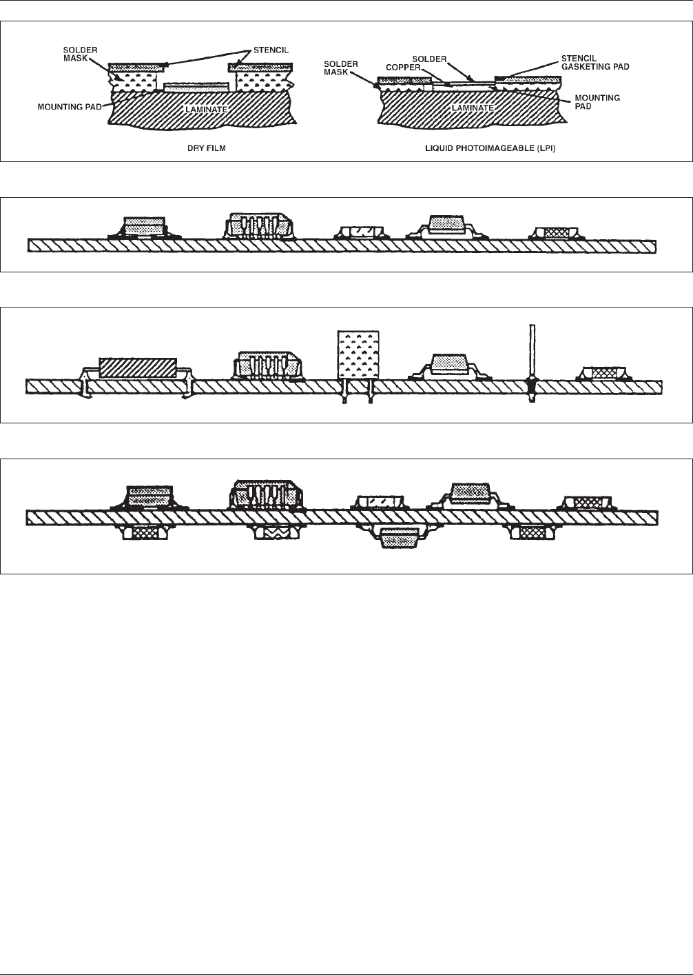
6.1.2 Solder Mask Thickness Issues Regardless of the
type of solder mask used for surface mount applications,
the solder mask must be the correct thickness and consis-
tent. Solder mask plays an important role in forming a gas-
ket between the solder paste stencil and the printed board
to reduce the extrusion of paste and limiting smearing.
Typical dry film solder masks range from 75 to 100 µm
thick, leaving the mask higher than the surface mount pads
(see Figure 6-1). Thus, the stencil will rest on the solder
mask and leave a gap between the stencil and the pads
through which solder paste can flow. However, typical liq-
uid photoimageable masks range from 15 to 30 µm thick.
This makes the pad surfaces the highest points on the board
so that when the stencil is lowered, it will rest on the pads.
The stencil then gaskets the opening around the pads, pre-
venting the solder paste from getting under the stencil.
Excessively thick solder mask, particularly dry film over
traces under components with small clearance, can contrib-
ute to the formation of crevices which entrap flux. In the
case where the solder mask touches the bottom of the com-
ponent, if insufficient solder paste is used, it may result in
chip component drawbridging (tombstoning), insufficient
solder fillet or lack of solder joint. (See IPC-SM-782 and
IPC-D-275)
Solder joint reliability under temperature cycling or power
cycling conditions may be reduced if the solder mask
touches the bottom of the component or conformal coating
filling the printed board-component gap. (See IPC-SM-
785.)
6.2 Temporary Solder Mask and Tapes Temporary sol-
der mask and tapes are used to prevent solder and solvents
from causing problems during assembly processes. In SMT
the reflow techniques may expose the mask or tape to tem-
peratures which may cause thermal breakdown. This may
cause reversion of some materials into a sticky ‘‘goo’’ and
others may adhere tenaciously making them difficult to
remove. The cleaning of SM assemblies may also be more
aggressive than through-hole. It is necessary to verify that
the temporary mask selected is compatible with the assem-
bly processes.
6.3 Conformal Coatings The primary purpose of confor-
mal coatings is to provide environmental protection. Some
conformal coatings have been shown to significantly affect
the reliability of surface mount solder joints. Parylene
(trademark of Union Carbide, chemical name Polyparaxy-
lylene) and silicone conformal coating have been shown to
improve accelerated fatigue life of SM solder joints by
approximately a factor of two or three. However in thermal
shock, some silicone coatings have been reported to
decrease life in thermal shock.
7.0 ASSEMBLY PROCESSES AND DESIGN FOR MANU-
FACTURABILITY
While there are only a few processes used in fabricating an
assembly with SMT components, these processes directly
impact the formation of the solder joint that provides the
reliable attachment of the part to the substrate. It is essen-
tial that the designer of surface mount assemblies under-
stand the manufacturing processes involved, including their
impact on the reliability of the completed assembly. Design
for manufacturability requires that the designer have a clear
view of the impact and limitations of the fabrication steps.
IPC-CM-770, Printed Board Component Mounting,
includes the following classification scheme for surface
mount assemblies:
Type 1 —Components (mounted) on only one side of
Table 6−1 Solder Mask Guidelines
RECOMMENDED FOR THESE SM SOLDERING
PROCESSES
SOLDER MASK TYPE
APPLICATION
METHOD THICKNESS
TENTED
VIAS
STANDARD
PITCH
REFLOW
FINE
PITCH
REFLOW
WAVE
SOLDER
Liquid Screenprint 8-50 µm N* N N N
Dry Film Hot roll Lamination 60-100 µm Y Y N Y
Liquid Photoimageable Open Screen Coat
Curtain Coat
Roller Coat
Electrostatic Spray
15-30 µm N Y Y Y
Combination (liquid
photoimageable* dry
film cap layer)
Lamination 50-75 µm Y N Y
*The majority of via holes can be filled by this process but not tented.
IPC-D-279 July 1996
24
the board
Type 2 —Components (mounted) on both sides of the
board
Class A —Through-hole component mounting only
Class B —Surface mounted components only
Class C —A mixture of through-hole and surface
mounting
The typical assembly with surface mount components on
only one side of the substrate (Type 1B - Figure 7-1) is
assembled by one of the following sequences:
1. Apply adhesive, place SM components, cure adhe-
sive, wave solder, clean, test/repair.
or;
2. Apply solder paste, place SM components, reflow
solder paste, clean, test/repair.
If the assembly contains both surface mount and through-
hole components of a single-sided assembly (Type 1C Fig-
ure 7-2), it may be assembled using one of the following
sequences:
1. Apply adhesive, place SM components, cure adhe-
sive, wave solder, clean, insert through-hole compo-
nents and clinch, wave solder, clean, test/repair.
or;
2. Apply solder paste, place SM components, reflow
solder paste, clean, insert through-hole components
and clinch, wave solder, clean, test/repair.
When only surface mount components are mounted on
both sides of an assembly (Type 2B - Figure 7-3), there are
typically two assembly options:
1. Apply solder paste to side 2 (bottom), place SM
components, reflow solder paste, clean, invert board,
apply solder paste to side 1 (top), reflow solder paste,
clean, test/repair.
IPC-279-06
Figure 6−1 Impact of Solder Mask Thickness on Stenciling
IPC-279-07
Figure 7−1 Type 1B Assembly − All SMT Components
IPC-279-08
Figure 7−2 Type 1C Assembly − Mixed Technology Assembly
IPC-279-09
Figure 7−3 Type 2B − All SMT Components
July 1996 IPC-D-279
25