IPC-D-279 EN.pdf - 第56页
beyond Class 2 requirements is the reliability diminished. However , solder joints not properly wetted, can prema- turely fail both as the result of mechanical and thermal cyclic loading [Refs. A-9: 1,31]. V oids in the …
protect the solder joints from expansion mis-
matches;
(3) Reduces solder joint strength because of weaker
solder/Alloy 42 interfacial bond (see Section
A-3.3);
(4) Reduces solderability (see Section A-3.4).
These potential reliability-threats can be avoided with the
choice of a copper lead frame; however, this requires a soft
die attach and the reversion to higher CTE molding com-
pounds for the components [Ref. A-9: 31].
A-6.0 VALIDATION AND QUALIFICATION TESTS
The validation and qualification tests should follow the
guidelines given in IPC-SM-785, Guidelines for Acceler-
ated Reliability Testing of Surface Mount Solder Attach-
ments.
However, for large components with significant heat dissi-
pation and small global CTE-mismatches, temperature
cycling tests are inadequate to provide the required infor-
mation; full functional cycling—including external tem-
perature and internal power cycling—is necessary.
A-7.0 SCREENING PROCEDURES
A-7.1 Solder Joint Defects
The solder joint defects of greatest reliability concern are
those involving inadequate wetting for whatever reason.
Well wetted solder joints, regardless of their geometric
variations within the standards provided by IPC-A-620,
Acceptability of Electronic Assemblies with Surface Mount
Technologies and ANSI/J-STD-001, Requirements for Sol-
dered Electrical and Electronic Assemblies, and somewhat
beyond, will not pose a reliability threat due to inadequate
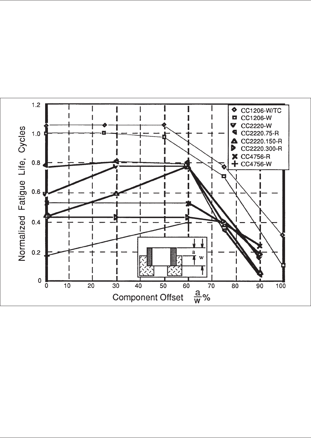
quality. In Figure A-3 the results of thermal cycling and
thermal shock tests are shown for solder joints of chip
components with a wide variety of component offsets and
overhangs.
Those solder joints have adequate strength even for severe
mechanical loading conditions as well as no diminished
thermal cyclic fatigue reliability. Only with severe offsets
Figure A−3 Effect of Component Offsets on the Fatigue Reliability of Three Capacitor Chip (CC) Sizes with −55<->+125°C
Thermal Shock or −20<->+100°C Thermal Cycling (TC) and Either Wave (W) or Reflow Soldered R) [Ref. A-9: 54,55]]. The
Lower Lives at Smaller Component Offsets Result from the Failure of the CC-Components not the Solder Joints. The
Fatigue Lives are Normalized, Since the Data are from Glued-Down CCs which Typically Exhibit Longer Solder Joint
Fatigue Lives than CCs not Glued-Down.
IPC-D-279 July 1996
44

beyond Class 2 requirements is the reliability diminished.
However, solder joints not properly wetted, can prema-
turely fail both as the result of mechanical and thermal
cyclic loading [Refs. A-9: 1,31].
Voids in the solder joints are generally regarded as not
constituting a reliability threat [Ref. A-9: 48]. Possible
exceptions are large voids reducing the solder joint cross-
section enough to reduce a required thermal heat transfer
function, and voids in high-frequency applications where
the voids can cause signal deterioration.
A-7.2 Screening Recommendations
Effective screening procedures need to be capable of caus-
ing the failure of latent solder joint defects, i.e., weak inad-
equately wetted solder joints, without causing significant
damage to high quality solder joints.
The best recommendation is random vibration (6-10 grams
for 10-20 minutes), preferably at low temperature, e.g.,
-40°C. This loading does not damage good solder joints,
but overstresses weakly bonded ones [Ref. A-9: 1].
Thermal shock can also be successfully used, however
some damage to good solder joints can be expected, par-
ticularly for larger components.
A-8.0 STEP-BY-STEP NUMERICAL EXAMPLE RELATING
REQUIRED DESIGN LIFE TO ACCELERATED RELIABIL-
ITY TEST RESULTS
This numerical example illustrates how the reliability of an
electronic system in the field can be assessed by using the
Design for Reliability (DfR) process in Appendix A or the
results of accelerated test results carried out as per IPC-
SM-785, Guidelines for Accelerated Reliability Testing of
Surface Mount Solder Attachments.
For example the following information is assumed:
Product:
Computer for Navy artillery—Use Category 6 in Table
A-1,
Design life = 10 years (= 3650 thermal cycles at 1 cycle/
day),
Component-external daily temperature cycles: 45 to 85°C
(∆T = 40°C) for 100 days/year and 25 to 85°C (∆T=
60°C) for 265 days/year (in the following text, the data
and results for these two loading conditions appear
before and after ‘‘//’’ respectively),
Acceptable cumulative failure probability at end of 10
years, x = 0.5%,
Largest leaded component:
68 I/O 50-mil pitch ceramic chip carrier (LCCC), α
C
= 6.3
ppm/°C (6.3x10
-6
/°C), dissipating 0.8 W raising the
component operating temperature to 93°C, with side-
brazed copper alloy compliant leads with a diagonal
lead stiffness of K
D
= 52 lb/in,
Largest leadless component:
CC1820 chip capacitor, α
C
= 6.8 ppm/°C,
Substrate:
Low CTE multilayer board, α
S
= 10.5 ppm/°C.
Reliability Estimates for Individual Components:
Ceramic Chip Carrier:
The input parameters into Eq. A-4 are: F = 1.0, K
D
=52
lb/in, L
D
= 0.674 in, ∆(α∆T) = 117.6x10
-6
//201.6x10
-6
(α
C
= 6.3 ppm/°C, α
S
= 10.5 ppm/°C, T
C
= 93°C, T
S
=
85°C, T
C,0
=T
S,0
= 45//25°C), A = 900x10
-6
in
2
,h=
0.005 in;
-> ∆D(leaded) = 5.459x10
-4
//1.604x10
-3
at ∆T = 40//60°C,
respectively.
The input parameters into Eq. A-2 are: T
SJ
= 67//57°C (T
C
= 93°C, T
S
= 85°C, T
C,0
=T
S,0
= 45//25°C), t
D
= 715
min;
-> c = −0.4751//−0.4691 at ∆T = 40//60°C, respectively.
Using these results in Eq. A-1 gives:
=> N
f
(50%) = 1,490,000//181,000 cycles at ∆T = 40//60°C,
respectively.
Using these results in Eq. A-8 with x = 0.5% and β =2
gives:
=> N
f
(0.5%) = 127,000//15,400 cycles at ∆T = 40//60°C,
respectively.
CC1820 Chip Capacitor:
The input parameters into Eq. A-3 are: F = 0.7, L
D
= 0.080
in, ∆(α∆T) = 148.0x10
-6
(α
C
= 6.8 ppm/°C, α
S
= 10.5
ppm/°C, T
C
= 85°C, T
S
= 85°C, T
C,0
=T
S,0
= 45//25°C),
h = 0.005 in;
-> ∆D(leadless) = 1.658x10
-3
//2.486x10
-3
at ∆T = 40//
60°C, respectively.
The input parameters into Eq. A-2 are: T
SJ
= 65//55°C (T
C
= 85°C, T
S
= 85°C, T
C,0
=T
S,0
= 45//25°C), t
D
= 715
min;
-> c = −0.4739//−0.4679 at ∆T = 40//60°C, respectively.
Using these results in Eq. A-1 gives:
=> N
f
(50%) = 148,000//73,000 cycles at ∆T = 40//60°C,
respectively.
Using these results in Eq. A-8 with x = 0.5% and β =4
gives:
=> N
f
(0.5%) = 43,000//21,000 cycles at ∆T = 40//60°C,
respectively.
Cumulative Damage Ratios for Multiple Cyclic Loads
The input parameters into Eq. A-10 are: N(∆T = 40//60°C)
= 1000//2650 cycles, N
f
(0.5%, LCCC, ∆T = 40//60°C)
= 127,000//15,400 cycles, N
f
(0.5%, CC1820, ∆T = 40//
60°C) = 43,000//21,000 cycles,
=> CDR(0.5%, LCCC) = 0.18 and CDR(0.5%, CC1820) =
0.15.
Reliability Estimates for Product with Multitude of Compo-
nents:
The input parameters into Eq. A-11 are: x = 0.5%, N(∆T=
July 1996 IPC-D-279
45
40//60°C) = 1000//2650 cycles, n(LCCC) = 30,
N
f
(0.5%, LCCC, ∆T = 40//60°C) = 127,000//15,400
cycles, β(LCCC) = 2, n(CC1820) = 100, N
f
(0.5%,
CC1820, ∆T = 40//60°C) = 43,000//21,000 cycles,
β(CC1820) = 4;
=>F
∑
(N = 3650) = 0.5%.
Thus, this design would just meet the reliability require-
ment of x ≤0.5% at the end of 10 years of service.
Accelerated Testing:
Test Components:
8 chip carriers (LCCC), 68 I/O 50-mil, α
C
= 6.3 ppm/°C
(measured), internally daisy-chained to allow indepen-
dent monitoring of each LCCC side (
1
⁄
4
of LCCC), with
side-brazed copper alloy compliant leads with a diago-
nal lead stiffness of K
D
= 52 lb/in (calculated), 256 chip
capacitors CC1820, α
C
= 6.8 ppm/°C (measured), with
metallization caps shorted with conductive epoxy on
capacitor top,
Test Substrate:
FR-4 multilayer board, α
S
= 16.0 ppm/°C (measured)
for greater CTE-mismatches and greater test accelera-
tion, test printed board lay-out provides for independent
continuity monitoring of each side of each chip carrier
(LCCC) and for continuity monitoring of groups of 8
chip capacitors (CCs) daisy-chained together. Confor-
mal Coating: Test vehicles are not conformally coated.
Test Parameters:
Temperature cycling from 0°C to 100°C at 24 cycles/
day, t
D
= 15 min, ∆T = 100°C and T
SJ
= 50°C.
Results of Accelerated Reliability Test:
N
f
(50%) = 982 and 6310 accelerated cycles-to-failure for
the individual LCCC sides and the 8 daisy-chained
CC1820s, respectively. Applying the partition correction
from Equation 16 in IPC-SM-785 results in N
f
(50%) =
491 and 10612 accelerated cycles-to-failure for the
actual LCCC and the CC1820 component attachments,
respectively.
Reliability Estimates by Extrapolation of Accelerated Test
Results:
Ceramic Chip Carrier:
The input parameters into Eq. A-4 are for the test: F =
1.0, K
D
= 52 lb/in, L
D
= 0.674 in, ∆(α∆T) = 970.0x10
-6
(α
C
= 6.3 ppm/°C, α
S
= 16.0 ppm/°C, T
C
=T
S
= 100°C,
T
C,0
=T
S,0
= 0°C), A = 900x10
-6
in
2
, h = 0.005 in;
-> ∆D(test) = 3.714x10
-2
.
and for the field use: F = 1.0, K
D
= 52 lb/in, L
D
= 0.674 in,
∆(α∆T) = 117.6x10
-6
//201.6x10
-6
(α
C
= 6.3 ppm/°C, α
S
= 10.5 ppm/°C, T
C
= 93°C, T
S
= 85°C, T
C,0
=T
S,0
=
45//25°C), A = 900x10
-6
in
2
, h = 0.005 in;
-> ∆D(use) = 5.459x10
-4
//1.604x10
-3
at ∆T = 40//60°C,
respectively.
The input parameters into Eq. A-2 are for the test: T
SJ
=
50°C (T
C
=T
S
= 100°C, T
C,0
=T
S,0
= 0°C), t
D
=15
min;
-> c(test) = −0.4160;
and for the field use: T
SJ
= 67//57°C (T
C
= 93°C, T
S
=
85°C, T
C,0
=T
S,0
= 45//25°C), t
D
= 715 min;
-> c(use) = −0.4751//−0.4691 at ∆T = 40//60°C, respec-
tively.
Using these results in Eq. A-12 in IPC-SM-785 with
N
f
(test, 50%) = 491 cycles gives:
=> N
f
(use, 50%) = 1,500,000//183,000 cycles at ∆T = 40//
60°C, respectively.
CC1820 Chip Capacitor:
The input parameters into Eq. A-3 are for the test: F =
0.7, L
D
= 0.080 in, ∆(α∆T) = 920.0x10
-6
(α
C
= 6.8
ppm/°C, α
S
= 16.0 ppm/°C, T
C
=T
S
= 100°C, T
C,0
=
T
S,0
= 0°C), h = 0.005 in;
-> ∆D(test) = 1.030x10
-2
.
and for the field use: F = 0.7, L
D
= 0.080 in, ∆(α∆T) =
148.0x10
-6
//222.0x10
-6
(α
C
= 6.8 ppm/°C, α
S
= 10.5
ppm/°C, T
C
=T
S
= 85°C, T
C,0
=T
S,0
= 45//25°C), h =
0.005 in;
-> ∆D(use) = 1.658x10
-3
//2.486x10
-3
at ∆T = 40//60°C,
respectively.
The input parameters into Eq. A-2 are for the test: T
SJ
=
50°C (T
C
=T
S
= 100°C, T
C,0
=T
S,0
= 0°C), t
D
=15
min;
-> c(test) = −0.4160;
and for the field use: T
SJ
= 65//55°C (T
C
=T
S,0
= 85°C,
T
C,0
=T
S,0
= 45//25°C), t
D
= 715 min;
-> c(use) = −0.4739//−0.4679 at ∆T = 40//60°C, respec-
tively.
Using these results into Eq. A-12 in IPC-SM-785 with
N
f
(test, 50%) = 10,612 cycles gives:
=> N
f
(use, 50%) = 148,000//73,000 cycles at ∆T = 40//
60°C, respectively.
Cycles-To-Failure for Daisy-Chains
Failure
No.
12345678
1
⁄
4
LCCC 146 196 388 418 486 540 568 628
8 CC1820 2718 3463 3826 4161 4397 4631 4738 5022
Failure
No.
9 10111213141516
1
⁄
4
LCCC 676 684 690 820 850 878 902 926
8 CC1820 5206 5372 5489 5598 5823 5978 6073 6223
Failure
No.
17 18 19 20 21 22 23 24
1
⁄
4
LCCC 1038 1044 1096 1122 1206 1214 1298 1350
8 CC1820 6397 Test terminated at 6,400 cycles
Failure
No.
25 26 27 28 29 30 31 32
1
⁄
4
LCCC 1386 1480 1536 1602 1716 1840 2002 2432
8 CC1820 Test terminated at 6,400 cycles
IPC-D-279 July 1996
46