IPC-D-279 EN.pdf - 第22页
Appendix J) to reduce evaluation time and cost c) corrosion avoidance - pertinent cleaning, component clearance and conductor spacing issues (see Appen- dices E, L and N and section 7.5, 7.8) d) control of electrical tra…

residues if they dissolve into the polymeric material during
the soldering and/or cleaning processes.
3.1.15 Solvent Compatibility Surface Mount printed
wiring Assemblies (PWA) are subjected to solvents (includ-
ing water) and chemicals during manufacture, rework,
repair and service. These agents include those used in sol-
dering (alcohols, glycols and other solvents in flux vehicles
at temperatures approaching 150°C), in cleaning the assem-
bly after solder (saponifiers, neutralizers, hot water, ter-
pene, mixtures, hydrochlorofluorocarbon (HCFC) mixtures
and other halogenated solvents and blends at moderate pro-
cess temperatures), during removal of conformal coatings
with various chemicals, and during service (hydraulic and
cooling fluids and fuels in military applications; alcohols
and halogenated hydrocarbons during cleanup). These sol-
vents and chemicals can adversely affect the solder mask
(SM), printed wiring board, conformal coating, printed
board or component legends and markings as well as
degrade thin or mechanically stressed sections of plastic
components. See Appendix I.
3.1.16 Corrosion The result of corrosion is material loss
of the metallic conductors, permanent or intermittent con-
tinuity loss due to build up of non-conductive corrosion
residues (particularly between contacts) and permanent or
intermittent shorts due to build up of conductive corrosion
residues and conductive metal dendrites. Corrosion accel-
erates the failure of components under cyclic fatigue con-
ditions.
The oxides of tin, nickel and copper are not good conduc-
tors. Low interfacial pressure contacts to these metals can
become resistive or intermittent. See Appendix L for
details.
3.1.17 External Radiation External radiation typically
includes X-Rays, β-particles and cosmic rays. It affects the
semi-conductor material through the generation of hole-
electron pairs in the bulk of the device. The purpose of
understanding the radiation effects is to enable the develop-
ment of radiation-hardened devices.
External radiation affects the different semiconductor
devices in different ways. For instance in bipolar types,
radiation causes an increase in low-frequency noise, high
leakage current across the p-n junctions, and a reduction in
current gain; in MOS types, a threshold voltage shift, a
reduction in transconductance and an activation of parasitic
elements are observed. See Appendix E.
3.1.18 Space Environment The space environment pre-
sents an unusual set of conditions which requires careful
evaluation (low air pressure, low gravity, low temperature
and radiation). See Appendix O.
3.2 Thermal Design The primary thermal parameter
which the designer must address is the temperature of the
junction or active film of the component; both the absolute
maximum or peak temperature and the steady state operat-
ing temperature limits imposed by the component manu-
facturer (as modified by derating protocols) must be
observed. The secondary thermal parameter is the solder
joint temperature since long service times at high tempera-
tures will result in grain growth in the solder, growth of the
intermetallic compound layers; and large temperature
swings in service will subject the joint to conditions lead-
ing to cyclic fatigue. See Appendix D for details.
Variation of the external (outside of the equipment enclo-
sure) ambient temperature is one of the multitude of factors
that will determine the actual temperature cycle a specific
surface mounted device will see in operation. Very simple
equipment, powered continuously at constant power will
see the same temperature swings as the external ambient.
In some cases, the system designer introduces built-in
means of reducing the temperature swing inside the cabi-
net, such as fans activated when the inlet air temperature
exceeds certain limits or inlet air heaters which are
activated when inlet air temperature drops below certain
limits.
In many applications, the variation of the temperature
inside the electronic enclosure is generated by variations of
the power dissipated by the electronics itself. Examples of
this type of behavior are on/off periods for the systems, and
fluctuations in the power dissipation as in telecommunica-
tion equipment due to variations in the number of simulta-
neous calls passing through the system.
It follows that different devices inside the same system
might be subjected to very different temperature cycles. In
order to assess the reliability of the solder joints, the
designer must perform a complete thermal analysis at the
device level.
In most applications, the temperature variations at a par-
ticular component in a system result from a combination of
system-external and system-internal temperature variations
combined with power dissipation fluctuations within the
component.
3.3 Printed Board Design and Layout The printed board
design and layout task, particularly for surface mount tech-
nology (SMT), has become more difficult and complex.
The difficulty of SMT designs has increased with the
increase in conductor density as a result of decreases in
termination pitch, conductor width and conductor spacing.
The complexity of SMT designs has increased with the
need to consider:
a) thermo-mechanical effects such as solder joint reli-
ability (see section 3.4, 3.6 and Appendix A)
b) testability and inspectability (see section 8 and
IPC-D-279 July 1996
10

Appendix J) to reduce evaluation time and cost
c) corrosion avoidance - pertinent cleaning, component
clearance and conductor spacing issues (see Appen-
dices E, L and N and section 7.5, 7.8)
d) control of electrical transients which become more
severe with the increased speeds and power density
of SMT designs. (See section 3.1 and Appendix E
and the issues of increase in ‘‘ground bounce’’ and
signal reflection noise.)
e) thermal design and control of the critical junction and
solder joint temperatures (see section 3.2 and Appen-
dices A, B, D and E)
f) manufacturability for high yield/quality assemblies
(see section 7.8 and Appendix K) including orienta-
tion, solder thiefs
g) ESD susceptibility mitigation of components through
a combination of layout and software. (See Appendix
H)
h) Component placement and orientation for enhanced
robustness to flexing, vibration and shock during the
assembly process as well as in the use environment.
(See Appendix E) The significant IPC document for
this section is IPC-SM-782
i) the impact of the limited heat transfer available from
solder joint to internal heat ‘‘sinks.’’
3.3.1 Thermal Design and Layout Where there are ther-
mally sensitive components, heat dissipaters should gener-
ally be ‘‘downstream’’ in the air flow. Under certain condi-
tions of PWA geometry, component orientation and relative
component heights, turbulence may result in ‘‘recirculation
cells’’ conveying heat ‘‘upstream.’’
3.3.2 Thermal Design and Conformal Coating Reduced
heat extraction from the PWA (and increased junction tem-
peratures) may result if conformal coating covers heat con-
duction surfaces on the PWA edge or margin which mate
with heat sinks such as card-edge clamps and cold plates.
(See Appendix D)
3.3.3 Land Patterns Surface land patterns define the
sites where the components are to be soldered to the
printed wiring board. The design of land patterns is very
critical because it is the land pattern that not only deter-
mines the solder joint strength and hence the reliability of
solder joints but also impacts the solder defects, cleanabil-
ity, testability, and repair/rework. The very producibility or
the success of the printed board is dependent upon the land
pattern design.
There are certain general guidelines that one should
develop to cope with the variations in tolerances of compo-
nents. The selected vendor’s components must pass all
package qualification requirements. Standardization of
parts reduces the tolerances that the land pattern design
will have to support.
A second desirable requirement is that the land pattern
design be transparent to the soldering process to be used in
manufacturing. This will not only reduce the number of
land sizes in the CAD library but it will also be less con-
fusing for the CAD designer.
3.3.4 Balance About Neutral Axis Balanced conductor
plane distribution about the neutral axis results in a SM
printed board which does not ‘‘potato-chip’’ during the
high temperature exposures and results in reduced
mechanical stress on component bodies and on solder
joints.
3.3.5 Vias Via holes are used to connect surface mounted
component lands to conductor layers. They may also be
used as test targets for bed-of-nails type probes and/or
rework ports. Via holes may be tented if they are not
required for node testing or rework. When a via is used as
a test point it is required that the location of a test land be
found to match the standard grid of the test fixture.
Buried Via A plated-through hole connected to neither the
primary side nor the secondary side of a multilayer pack-
aging and interconnecting structure; i.e., it connects only
internal layers.
Blind Via A plated-through hole connected to either the
primary side or the secondary side and one or more inter-
nal layers of a multilayer packaging and interconnecting
structure.
IPC-TR-579 noted possible reliability problems for PTVs
with small diameters and/or large printed board thick-
nesses. Copper plating quality in the barrel was found to be
a significant parameter; nickel over plating in the barrel
increases the robustness of the PTV to temperature cycling.
Use of blind and buried vias can result in effective aspect
ratios (AR) much lower than the AR of PTVs in the same
substrate with the same diameter. See section 3.6.
Open or untented PTVs (no solder mask on either side of
the printed board) can allow liquid flux to be trapped with
potential for corrosion, reducing SIR, contaminating test
fixtures and causing electrochemical corrosion. (See IPC-
D-275) If solder mask is intended to plug or tent these
holes, it must do it consistently. Another method to prevent
flux from being trapped in these vias is to plug them with
solder (which wave soldering does automatically).
3.3.6 Printed Board Trace Widths and Spaces
Minimum trace widths should be reviewed keeping in mind
the influence of etching tolerances, undercutting, ‘‘Mouse-
bites,’’ and plated grain size as well as the possibility for
electromigration due to current density, Joule heating and
July 1996 IPC-D-279
11
subsequent conductor temperature rise.
Minimum trace spacings should be reviewed keeping in
mind the influences of DC voltage and possible electro-
chemical migration, AC voltage and possible corona leak-
age currents, high humidity and possible electrochemical
migration, low air pressure and possible corona leakage
currents/premature voltage breakdown, and conductive or
corrosive contamination from the ambient. See IPC-D-275,
IPC-SM-782, and IPC-TR-476 and IEC 664.
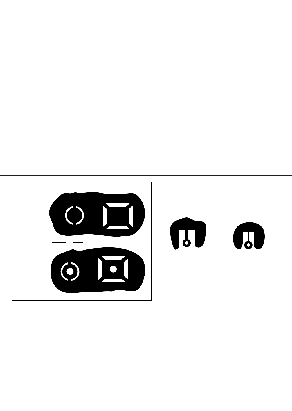
3.3.7 PTH and PTV Thermal Isolation/Relief Large con-
ductor areas such as ground planes, power planes and ther-
mal planes ‘‘heatsink’’ PTH and PTVs to which they con-
nect. During the soldering or reflow process, the reduction
in local temperature can result in ‘‘cold’’ solder joints,
bridging or icicling and may require increased time at tem-
perature to affect a proper and reliable solder joint. Ther-
mal relief inner lands such as those depicted in Figure 3-2
provide a measure of thermal resistance between the exter-
nal soldered lands and the heatsinking plane. The results
are lower required reflow temperatures, less printed board
stress, and more consistent solder joints.
3.3.8 Test Pads Test pads are required for bare-board
test; see also IPC-ET-652. Previous techniques used to
implement digital PWA testability such as massive addition
of test nodes, become less feasible with the smaller dimen-
sions of SMT PWAs and the number of test nodes required
for components with 100-400 terminations; the mechanical
force exerted by test pins is sufficient to flex and break
components and solder joints.
Testability is a particular issue for field repair activities
where the full capabilities of the SM PWA may not be
exercised due to test equipment limitations or lack of avail-
able test time; Built-in-Test-Equipment, Built-in-Test,
Built-in-Self-Test (BITE, BIT or BIST) capabilities could
be invaluable in these circumstances or may be the only
alternatives. See section 8 and Appendix J.
Solder mask overlap or residue on test pads (whether by
design or by loss of process control) reduces test reliabil-
ity. (See IPC-D-275, and IPC-SM-782)
Provide adequate margin between the land and solder
mask.
Conformal coating on test pads results in diminished test
accessibility; testability buss methodologies and structures
may be required to permit effective and efficient fault cov-
erage. (See IPC-SM-782)
3.3.9 Spacing Between Parts The designer should pro-
vide for manufacturability, inspectability, testability and
repairability of SMT assemblies. A minimum interpackage
spacing is required to satisfy all these manufacturing
requirements. Some designs require that surface mount
components be positioned as tightly as possible (brick-
walled); these designs do not allow solder joint inspection.
See figure 3-3 and section 8.0.
3.3.10 ‘‘Pads-Only’’ Design For this reason, many mul-
tilayer military and space applications utilize a ‘‘pads-
only’’ outer layer design. By submerging all conductors
and power planes in the inner-layers, only the land areas
are exposed on the board surface. Connection to the sub-
layers is then accomplished by small plated and filled vias
IPC-279-04
Figure 3−2 Thermal Relief in Ground Planes
Land Before
Drilling
Land
After Drilling
Wide Straps Narrow Straps
Web Width
▼
▼
IPC-D-279 July 1996
12