IPC-D-279 EN.pdf - 第126页
T able L−1 Galvanic Compatibility of Metals MET AL GROUP I GROUP II GROUP III GROUP IV ANODIC - Corroded Magnesium/Magnesium Alloys X Zinc/Zinc Plating X X Aluminum filled (silver plated) Elastomer die Cut Edge (-740) Alu…

between conductors or barrels pre- and post-assembly
process stresses. To break possible CAF paths, use a
minimum of 2 plies for all layers and smooth and seal
board edges.
• printed board supplier’s inspection area is controlled
for humidity, temperature, cleanliness. Volume resis-
tance is a strong function of temperature changes, sur-
face resistance (SIR) is a strong function of humidity
and humidity changes, and delamination/measling/
vesication are functions of laminate cleaning and
cleanliness.
L-6.1 Galvanic Corrosion See also Sections 4 and 9,
ASM Electronic Materials Handbook, Volume 1, Packag-
ing, 1989; Contamination Effects on Electronic Products by
Carl Tautscher, Marcel Dekker, Inc., 1991, ISBN 0-8247-
8423-5. For sources of Ecorr vs. SCE, see Galvanic and
Pitting Corrosion-Field and Lab Studies, ASTM STP 576,
1976
Caution
Aluminum - 1% Silicon - 0.5% Copper alloy used for inte-
grated circuit metallization contains Al
2
Cu (Q phase)
which has a large oxidation (galvanic) potential with
respect to aluminum; in the presence of moisture, rapid
oxidation of aluminum occurs in the vicinity of copper
precipitates - and pits grow in the aluminum.
IPC-D-279 July 1996
114
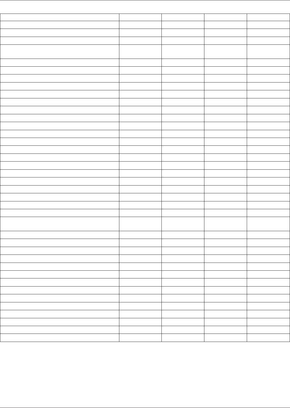
Table L−1 Galvanic Compatibility of Metals
METAL GROUP I GROUP II GROUP III GROUP IV
ANODIC - Corroded
Magnesium/Magnesium Alloys X
Zinc/Zinc Plating X X
Aluminum filled (silver plated)
Elastomer die Cut Edge (-740)
Aluminum/Aluminum alloys (-740 to -840 mV) X X
Beryllium X X
Chromium Plating X X
Tungsten X X
Molybdenum X X
Cadmium Plating (Restricted) X X
Carbon Steel, Cast Iron X X
Stainless Steel, Active X X
Lead, Tin-Lead Solder X X
Tin/Tin Plating (-440 V) X X
Tin/Indium X X
Nickel/Nickel Plating, Active (-250 mV) X X
Leaded Brass/Bronze X X
Copper-Zinc Alloys (Brasses)
Naval Brass X X
Brass, Commercial Yellow XX
Copper/Copper Alloys (-244 mV) X X
Beryllium Copper XX
Copper-Tin Alloys (Bronzes)
Copper-Nickel Alloys XX
Aluminum or copper filled (silver plated)
Elastomer (-190 to -200 mV)
Monel (-125 mV) XX
Silver Solder XX
Nickel, Nickel Plating, Passive X X
Cobalt, Cobalt/Nickel alloy XX
Stainless Steel, Passive XX
Silver-filled Elastomers (-50 mV) X
Silver/Silver alloys (-25 mV) X
Silver-filled Films X
Graphite/Carbon X
Rhodium X
Palladium X
Titanium X
Gold, Platinum, Gold/Platinum Alloys X
CATHODIC - Protected X
July 1996 IPC-D-279
115

Appendix M
Solder Joint Variability
M-1.0 SOLDER JOINT VARIABILITY
Appendix A describes the design parameters which deter-
mine the mean cycles to failure. The Weibull parameter
describes the variability in the response of the solder
attachment and the individual solder joints due to manufac-
turing or processing conditions as well as the inherent vari-
ability in wear-out processes.
• Open surface mount solder joints have been found
after a period in service. These ‘‘cold’’ or ‘‘dry’’ solder
joints were characterized by a component termination
and substrate land which were mechanically touching
but not completed with a permanent solder connection
with intermetallic compound (IMC) formation can
open during service. Tin-lead to tin-lead mechanical
contacts (under light mechanical loading and not sol-
dered) oxidize and open in service under temperature
cycling or vibration/shock conditions. This failure
mode is similar to the ‘‘fretting corrosion’’ described
in these appendices.
Failed joints have been traced to
• planarity (or coplanarity) problems on the component
termination
• planarity (or coplanarity) problems on the substrate
land
• solderability problems on the component termination
and on the substrate land
• improper selection of solder paste/flux.
• improper solder reflow processing.
Difficulty in inspection has resulted in ‘‘dry’’ solder joints
that are seen on J-lead solder joints. These ‘‘dry’’ joints are
insidious because they can be intermittent and be reported
as ‘‘NTF;’’ however, gull-wing terminations are not
exempt. Gull-wing leads are preferable to J-leads only
because they are not hidden under the component and sol-
der joints can be inspected and reworked more easily.
Some solder joints to gull-wing terminations have been
found to be open due to excessive IMC formation and
mechanical disturbance during solder solidification. Some
companies use an electric or air driven plunger to ‘‘tap’’
PWAs during functional test to detect ‘‘cold’’ or ‘‘dry’’ sol-
der joints. Some repair technicians use a pencil ‘‘tapper’’ to
detect these solder joints. ‘‘3D’’ optical or X-Ray systems
may be fast enough and definitive in their detection of
defective joints.
• for the ideal SM solder joint of uniform thickness (for
minimum dispersion in the Nf or cycles to failure), the
surface of the solder paste on the lands of the printed
board must be coplanar (in the same plane), all the
leads of the SMT component must also be coplanar
and contact the solder paste simultaneously. If there is
a gap between any lead and the solder paste, a defec-
tive joint is likely.
Coplanarity and solder volume issues include:
• Maintenance of component lead coplanarity requires
appropriate shipping and storage containers, such as
trays rather than tubes for Ceramic Leaded Chip Car-
riers to prevent lead interlocking and damage and stor-
age of parts to be used for repair/rework or ‘‘kitting’’
in the original container rather than loosely ‘‘binning’’
them,
• Some of the requirement for perfect coplanarity is alle-
viated because the component leads sink into the sol-
der paste and into the molten solder; this requires that
cumulative coplanarity (between the substrate and the
component leads) apply over the dimension of the
component to ~100 µm. Solder paste thickness for
Fine Pitch and extra Fine Pitch (FP, XFP) is less than
that for the coarser pitch of 0.5 - 1.2 mm components
and therefore the cumulative coplanarity requirement
is tightened to ~75 µm, again over the dimension of
the component.
Large, uninterrupted stencil openings result in thin
paste in the middle of the opening; paste uniformity is
aided by assembling the large opening from a multi-
plicity of narrower openings with the long axis paral-
lel to squeegee blade travel.
• Planarity of the substrate lands is lost, particularly in
the case of Fine Pitch and extra Fine Pitch (FP, XFP),
when the substrate is processed through hot air solder
leveling or hot air leveling (HASL or HAL). These
processes leave uneven deposits of solder on the pads
with the distribution often a function of the location of
the pad on the panel.
• The volume of solder in the joints can be reduced by
via and feedthrough holes/pads, as well as large area
conductors or other large lands very close to compo-
nents lead pads; these features tend to draw solder
away from (steal or thieve) the intended solder joint
and should be covered with solder mask or separated
with narrow conductors, covered or not with solder
mask. The presence of a large number of solder balls
or a number of large solder balls also indicates a
reduction in the solder available for joints.
• The ideal SM solder joint is metallurgically joined to
the component lead and to the substrate land with no
voids in the joint nor sign of non-wetting or dewetting
IPC-D-279 July 1996
116