IPC-D-279 EN.pdf - 第54页
A-5.2 Area Arrays (BGA, CGA) Grid array components (GACs) come in a variety of styles and materials. The major variations are BGAs, available with plastic bodies as PBGAs or ceramic bodies as CBGAs, and solder attached w…

where
F
∑
(N) = system cumulative failure probability after N
total cycles,
n
i
= number of components of type i,
N
i,j
= actual number of cycles applied to component
i at a specific cyclic load level j,
N
f,i,j
(x%)= fatigue life of solder attachment of component
i at load level j at x% failure probability,
β
i
= Weibull slope for SM solder attachment of
component i.
A-4.0 DfR-PROCESS
Appropriate DfR-measures to improve reliability can take
one of two forms, which are best employed in combination
for improved reliability margins. These measures are:
1) CTE-tailoring to reduce the global expansion mis-
match;
2) Increasing attachment compliancy, e.g., by
increasing the solder joint height, to accommodate
the global expansion mismatch;
3) Underfilling the gap between the component and
substrate;
Further, a DfR procedure aiming at high-reliability should
also include
4) Choosing base materials that have not too large a
local CTE-mismatch with solder, or
5) In case item (4) cannot be done, reduce the con-
tinuous wetted length to reduce interfacial
stresses.
CTE-tailoring involves choosing the materials or material
combinations of the MLB and/or the components to
achieve an optimum ∆CTE. An optimum ∆CTE for active
components dissipating power is ~1-3 ppm/°C (depending
on the power dissipated) with the MLB having the larger
CTE, and 0 ppm/°C for passive components. Of course,
since an assembly has a multitude of components, full
CTE-optimization cannot be achieved for all
components—it needs to be for the components with the
largest threat to reliability. For military applications with
the requirement of hermetic—and thus ceramic—
components, CTE-tailoring has meant the CTE-
constraining of the MLBs with such materials as Kevlar
TM
and graphite fibers, or copper-Invar-copper and copper-
molybdenum-copper planes. Such solutions are too expen-
sive for most commercial applications for which glass-
epoxy or glass-polyimide are the materials of choice for the
MLBs. Thus, CTE-tailoring has to take the form of avoid-
ing larger size components that are either ceramic (CGAs,
MCMs), plastic with Alloy 42 leadframes (TSOPs, SOTs ),
or plastic with rigid bonded silicon die (PBGAs).
Increasing attachment compliancy for leadless solder
attachments means increasing the solder joint height (C4,
C5, shimming, gluing [Refs. A-9: 42,43], 10Sn/90Pb balls,
10Sn/90Pb columns) or switching to a leaded attachment
technology. For leaded attachments, increasing lead compli-
ancy can mean changing component suppliers to those hav-
ing lead geometries promoting higher lead compliancy or
switching to fine-pitch technology.
The DfR-process needs to emphasize a physics-of-failure
perspective without neglecting the statistical distribution of
failures. The process might involve the following steps:
A. Identify Reliability Requirements—expected
design life and acceptable cumulative failure
probability at the end of this design life;
B. Identify Loading Conditions—use environments
(e.g., IPC-SM-785) and thermal gradients due to
power dissipation, which may vary and produce
large numbers of mini-cycles (Energy Star);
C Identify/Select Assembly Architecture—part and
substrate selections, material properties (e.g.,
CTE), and attachment geometry;
D. Assess Reliability—determine reliability potential
of the designed assembly and compare to the reli-
ability requirements using the approach shown
here, a ‘Figure of Merit’-approach [Ref. A-9: 44],
or some other suitable technique; this process may
be iterative;
E. Balance Performance, Cost and Reliability
Requirements.
A-5.0 CRITICAL FACTORS FOR EMERGING ADVANCED
TECHNOLOGIES
The lessons learned over the past 15 years with surface
mount technology (SMT) and fine-pitch attachments
should be heeded and applied. However, some of the
emerging advanced technologies fall outside the previous
experience with SMT attachments. It is therefore important
that appropriate design validation and qualification tests be
carried out to extend and, if necessary, alter and augment,
the existing understanding.
Following are short descriptions of some new technologies
where DfR, particularly for the solder attachments, is of
prime concern.
A-5.1 Flip Chip on Laminate
Here the biggest reliability concern is the large expansion
mismatch between the chip silicon and the polymeric sub-
strate. This either means relatively small chips or the use of
organic underfill materials which relieve the solder joints
from most of the thermal expansion mismatch loads. The
underfill material does however make repairs difficult if not
impossible. Detailed information about this technology has
been assembled in ANSI/J-STD-012, Implementation of
Flip Chip and Chip Scale Technology.
IPC-D-279 July 1996
42

A-5.2 Area Arrays (BGA, CGA)
Grid array components (GACs) come in a variety of styles
and materials. The major variations are BGAs, available
with plastic bodies as PBGAs or ceramic bodies as
CBGAs, and solder attached with either the C5-process or
with solder joints containing 10Sn/90Pb solder balls; and
CGAs with 10Sn/90Pb solder columns.
The long-term reliability of the solder attachments to FR-4
printed boards is a big concern with GACs. The global
thermal expansion mismatch between the GACs and the
printed board can be quite large as the result of the combi-
nation of large GAC sizes, large differences between the
thermal expansion coefficients of the GACs and the printed
board (∆CTE), and the power dissipation within the GACs.
Further, depending on the die attach and the GA material,
a large localized global thermal expansion mismatch under-
neath the die and a significant local thermal expansion mis-
match between the solder itself and the GA surface can
increase the threat to reliability. In addition, the implemen-
tation of the Government-mandated ‘‘Energy Star’’ pro-
gram, the number of thermal cycles could be a multiple of
the once-a-day diurnal/on-off cycles.
The solder attachments of GACs vary depending on the
loading conditions to which the solder joints are subjected
to and the reliability requirements for the product. As men-
tioned earlier, BGAs are attached with either the
C5-process or with 10Sn/90Pb solder balls. The
C5-process, similar to the C4- or flip-chip-process, results
in solder joints heights that are less controlled and lower
{h~400 to 640 µm}, while the 10Sn/90Pb solder balls typi-
cally with diameters of 760 to 890 µm result in uniform
solder joint heights of the same dimension since the 10Sn/
90Pb solder has a liquidus temperature significantly above
the near-eutectic Sn/Pb solders and does not melt during a
typical reflow process. The solder columns, which cur-
rently are only used for ceramic GACs, are 10Sn/90Pb col-
umns with lengths of 1.25 to 2.30 mm that are either cast
onto the CGA or are wires soldered to both the CGA and
the substrate with near-eutectic Sn/Pb solder. The ratios of
fatigue lives, all parameters other than the solder joint
height being equal, are CBGA(0.40 mm): CBGA(0.75
mm): CGA(2.30 mm) = 1: 4: 45. The height of the solder
columns is limited by the requirement that the column
height-to-diameter aspect ratio does not produce slender
columns thus changing the loading conditions; cast col-
umns can accommodate larger aspect ratios.
It is also of importance for PBGAs, how the silicon chips
are attached to the BGA body. For ‘cavity-up’ components,
only a thin plastic layer separates the solder joints from the
die attach. As a consequence, the CTE underneath a rigid
die attach can be as low as 6 to 8 ppm/°C (very similar to
ceramic) locally raising the CTE-mismatch between the
PBGA and the FR-4 printed board from ∼2 to 10 ppm/°C.
Thus, the die size can only be ∼
1
⁄
5
the size of the BGA to
not negatively affect the reliability. Typically, die sizes are
significantly larger than that, with the result that the solder
joints at the comers of the die fail before the outermost
BGA corner joints. The larger the die, the worse the solder
attachment reliability [Refs. A-9: 45,46]. Thus, the trend
towards perimeter-PBGAs, where solder joints exist only
on the package perimeter—with the possible exception of
some thermal solder balls and vias in the package center—
for routing reasons, is beneficial for reliability [Ref. A-9:
47].
Further, the solder joint fractures are typically near the
interface between the BGA and the barrel-shaped solder
joints; this is a consequence of the contribution to the sol-
der joint loading of the local expansion mismatch between
the solder and the die-constraint BGA body [Ref. A-9: 45].
Substantial increases in fatigue life have reported with a
soft die attach [Ref. A-9: 48].
The geometry of the solder joints as well as the solder land
metallization have significant influence on the reliability.
The solder masks can have a negative influence if they are
used for solder mask-defined (SMD) lands with the solder
mask on the metallization lands affecting the solder joint
geometries. Stress concentrations created by the SMD-
solder joint geometries can be the origin of solder joint
failures and reduced reliability. For equal solder joint
height, increases in fatigue life by factors of about 1.25 to
3 can be anticipated with the use of non-solder mask-
defined (NSMD) vs. SMD lands with the larger improve-
ments for solder joints with the more severe loading con-
ditions [Refs. A-9: 46, 48-51].
For PBGAs the additional reliability issue of via and con-
ductor failures has surfaced [Ref. A-9: 52]. The former
issue is addressed in Section A-4 and the latter can be rem-
edied by wider conductors and/or better copper foil [Ref.
A-9: 53].
Detailed information about this technology has been
assembled in ANSI/J-STD-013, Implementation of Ball
Grid Array and Other High Density Technology.
A-5.3 Thin Packages (TSOP)
The biggest reliability issue regarding TSOPs (thin small
outline packages) stems from the choice of Alloy 42 for the
leadframe material by some component manufacturers
[Refs. A-9: 27-31]. This material choice has the following
consequences with regard to the solder attachment reliabil-
ity:
(1) Increases global CTE-mismatch, because compo-
nent CTE is reduced to about the CTE of ceramic;
(2) Increases lead stiffness due to higher modulus of
elasticity reducing the effectiveness of the leads to
July 1996 IPC-D-279
43
protect the solder joints from expansion mis-
matches;
(3) Reduces solder joint strength because of weaker
solder/Alloy 42 interfacial bond (see Section
A-3.3);
(4) Reduces solderability (see Section A-3.4).
These potential reliability-threats can be avoided with the
choice of a copper lead frame; however, this requires a soft
die attach and the reversion to higher CTE molding com-
pounds for the components [Ref. A-9: 31].
A-6.0 VALIDATION AND QUALIFICATION TESTS
The validation and qualification tests should follow the
guidelines given in IPC-SM-785, Guidelines for Acceler-
ated Reliability Testing of Surface Mount Solder Attach-
ments.
However, for large components with significant heat dissi-
pation and small global CTE-mismatches, temperature
cycling tests are inadequate to provide the required infor-
mation; full functional cycling—including external tem-
perature and internal power cycling—is necessary.
A-7.0 SCREENING PROCEDURES
A-7.1 Solder Joint Defects
The solder joint defects of greatest reliability concern are
those involving inadequate wetting for whatever reason.
Well wetted solder joints, regardless of their geometric
variations within the standards provided by IPC-A-620,
Acceptability of Electronic Assemblies with Surface Mount
Technologies and ANSI/J-STD-001, Requirements for Sol-
dered Electrical and Electronic Assemblies, and somewhat
beyond, will not pose a reliability threat due to inadequate
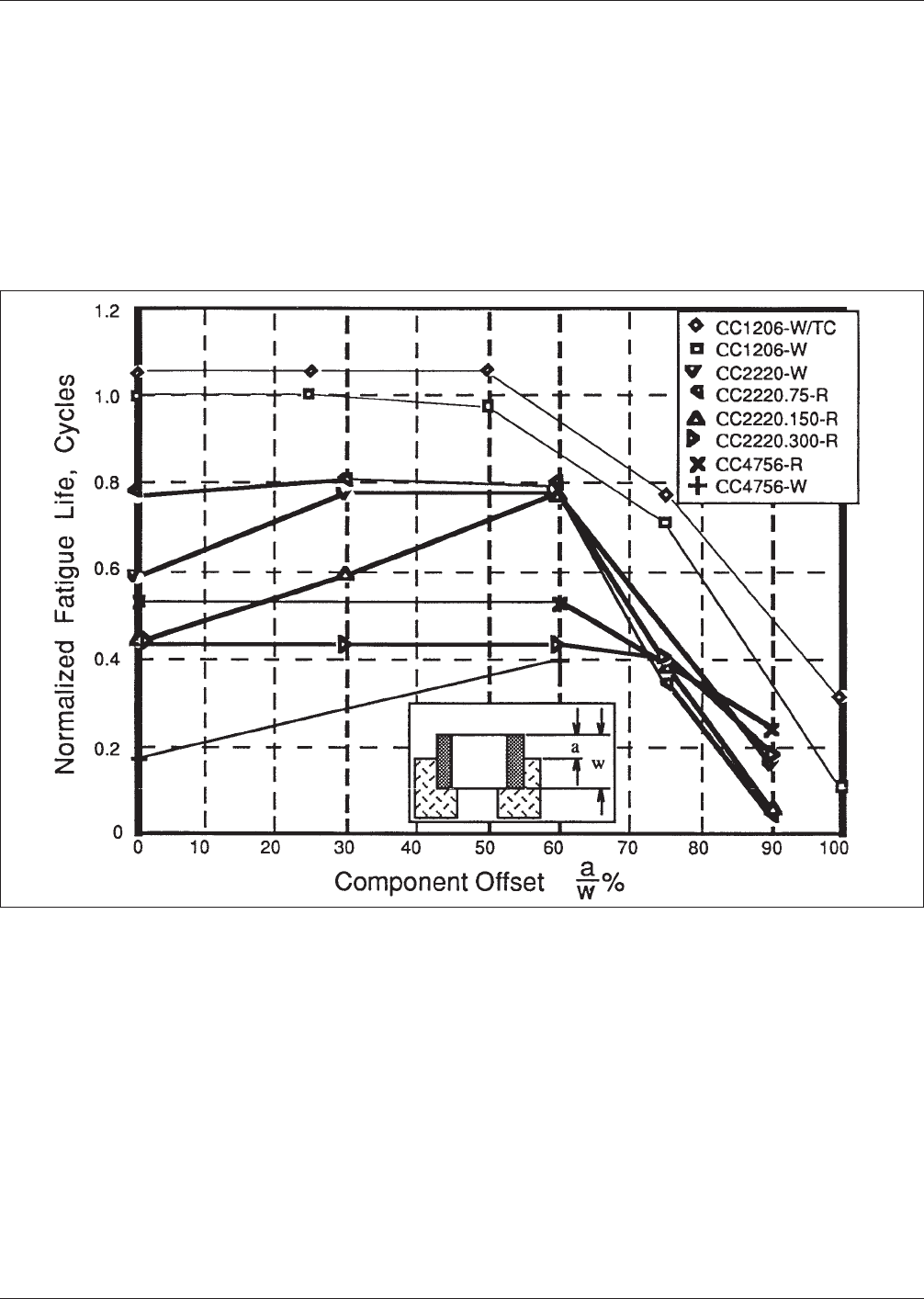
quality. In Figure A-3 the results of thermal cycling and
thermal shock tests are shown for solder joints of chip
components with a wide variety of component offsets and
overhangs.
Those solder joints have adequate strength even for severe
mechanical loading conditions as well as no diminished
thermal cyclic fatigue reliability. Only with severe offsets
Figure A−3 Effect of Component Offsets on the Fatigue Reliability of Three Capacitor Chip (CC) Sizes with −55<->+125°C
Thermal Shock or −20<->+100°C Thermal Cycling (TC) and Either Wave (W) or Reflow Soldered R) [Ref. A-9: 54,55]]. The
Lower Lives at Smaller Component Offsets Result from the Failure of the CC-Components not the Solder Joints. The
Fatigue Lives are Normalized, Since the Data are from Glued-Down CCs which Typically Exhibit Longer Solder Joint
Fatigue Lives than CCs not Glued-Down.
IPC-D-279 July 1996
44