IPC-D-279 EN.pdf - 第11页
T able A−2 Quality of Solder Joints with Copper and Alloy 42 Resulting from Different Reflow T emperatures...................................................... 38 T able B-1 Estimates of T ensile Properties of Copper Dep…

Appendix L Corrision Basics and Checklist
L-1.0 CORROSION BASICS
...................................... 111
L-2.0 CORROSION OF THE PWA............................. 111
L-3.0 CORROSION IN COMPONENTS..................... 111
L-4.0 OTHER EFFECTS OF WATER AND WATER
VAPOR
............................................................... 111
L-5.0 FRETTING ‘‘CORROSION’’.............................. 112
L-6.0 CORROSION DESIGN CHECKLIST................ 112
L-6.1 Galvanic Corrosion.......................................... 114
Appendix M Solder Joint Variability
M-1.0 SOLDER JOINT VARIABIALITY
..................... 116
Appendix N Adhesives, Solder Mask and Conformal/
Other Coatings
N-1.0 ADHESIVES
...................................................... 119
N-1.1 Electrically Conductive Attachment
Materials........................................................... 119
N-1.2 Thermally Conductive Adhesives.................... 119
N-1.3 Mechanical Attachment Adhesives.................. 119
N-2.0 SOLDER MASK................................................ 119
N-2.1 Types of Solder Masks.................................... 120
N-2.1.1 Liquid Screenprinted Solder Mask.................. 120
N-2.1.2 Dry Film........................................................... 120
N-2.1.3 Liquid Photoimageable.................................... 121
N-3.0 TEMPORARY MASKS AND STOPS............... 121
N-4.0 CONFORMAL COATING.................................. 121
N-4.1 Selection of Coating ....................................... 122
N-4.2 Thermal Stress Design Considerations ........... 122
N-4.3 Chemical Stress Design Considerations.......... 122
N-4.4 Space Environment Design Considerations.... 122
N-4.5 Manufacturing Considerations......................... 122
N-4.6 Other Design Considerations........................... 122
N-5.0 COMMON CRITICAL PROPERTIES OF
SOLDER MASK AND CONFORMAL
COATINGS
........................................................ 123
N-6.0 JUNCTION COATINGS, ‘‘GLOB-TOPS’’......... 124
Appendix O Aerospace and High Altitude Concerns
O-1.0 INTRODUCTION
............................................... 125
O-2.0 THERMAL DESIGN.......................................... 125
O-3.0 LARGE THERMAL EXCURSIONS.................. 125
O-4.0 CONTAMINATION ............................................ 125
O-5.0 RADIATION ENVIRONMENT........................... 126
O-6.0 ELECTRICAL PROPERTIES OF GASES....... 126
O-7.0 GRAVITY (OR LACK OF)................................ 126
Appendix P Technical Acronyms and Abbreviations
Figures
Figure 1−1
General Design Steps.......................................... 3
Figure 1−2
Flow Chart for Reliability Assurance Processes.. 4
Figure 3−1
SMT Assembly Response to Thermal Shock ...... 8
Figure 3−2
Thermal Relief in Ground Planes....................... 12
Figure 3−3
Spacing Between Parts...................................... 13
Figure 6−1 Impact of Solder Mask Thickness on
Stenciling............................................................ 25
Figure 7−1
Type 1B Assembly − All SMT Components....... 25
Figure 7−2 Type 1C Assembly − Mixed Technology
Assembly............................................................ 25
Figure 7−3
Type 2B − All SMT Components........................ 25
Figure 7−4
Type 2C − Mixed Technology............................. 26
Figure A−1 Depiction of the Effects of the Accumulating
Fatigue Damage in Solder
Joint Structure.................................................... 35
Figure A−2 Solder Joint Pull Strengths for Gullwing Leads
Consisting of Alloy 42 from Different Vendors
and Copper......................................................... 39
Figure A−3 Effect of Component Offsets on the Fatigue
Reliability of Three Capacitor
Chip (CC) Sizes ................................................. 44
Figure B−1 Cross-Section Schematic of a PTV With a
Barrel Fracture Near the Center of the MLB..... 52
Figure B−1 Cross-Section Schematic of a PTV With a
Barrel Fracture Near the Centerof the MLB ...... 52
Figure B−2 Schematic Cross-Sectional View of a PTV with
a Shoulder Fracture in a printed board.............. 53
Figure B−3 Reduction of Available Copper Ductility Due to
Localized Nicks Reducingthe Width of the
FlexCircuit Conductors [Ref. B-7: 25] and PTV
Stress Concentration Factor, K
c
......................... 56
Figure D−1
Thermal Vias and Planes................................... 70
Figure D−2
Other Methods of Conductive Heat Transfer..... 70
Figure D−3
Use of Heat Slug................................................ 71
Tables
Table 1−1
The Design Team................................................. 1
Table 3−1 Realistic Representative
(1)
Use Environments,
Service Lives, and Acceptable Failure
Probabilities for Surface Mounted Electronics
Attachments by Use Categories .......................... 6
Table 4−1 Advantages and Disadvantages of Various
Types of Substrates ........................................... 18
Table 6−1
Solder Mask Guidelines..................................... 24
Table A−1 Realistic Representative
(1)
Use Environments,
Service Lives, and Acceptable Failure
Probabilities for Surface Mounted Electronics
Attachments by Use Categories ........................ 35
IPC-D-279 July 1996
viii

Table A−2 Quality of Solder Joints with Copper and Alloy
42 Resulting from Different Reflow
Temperatures...................................................... 38
Table B-1 Estimates of Tensile Properties of Copper
Deposit Inside the PTVs .................................... 52
Table B−2 Estimates of the Fatigue Life and Time to
Failure of PTVs in Some Typical Use
Environments from Table A-1............................. 57
Table C−1
SIR Test Parameters for Some Industry Tests... 63
Table G−1 Typical Values for Coefficients of
Thermal Expansion (ppm/°C)............................. 96
Table G−2
Properties of Printed Circuit Laminates............. 98
Table K-1 Checklist for Design for Manufacturability and
Assembly.......................................................... 109
Table L−1
Galvanic Compatibility of Metals...................... 115
July 1996 IPC-D-279
ix
Design Guidelines for Reliable
Surface Mount Technology Printed Board Assemblies
1.0 SCOPE
This document establishes design concepts, guidelines, and
procedures intended to promote appropriate ‘Design for
Reliability (DfR)’ procedures and to ensure reliable printed
wiring assembly (PWA) characteristics. The major focus of
the information presented is directed toward those PWAs
that have surface mount (SM) components, either totally, or
intermixed with through-hole components, mounted on one
or both sides of the mounting structure.
1.1 Purpose The definition of reliability in this docu-
ment is:
Reliability is the ability of a product to function under
given conditions and for a specified period of time with-
out exceeding acceptable failure levels.
This document addresses reliability-related aspects of prod-
uct design, process design, as well as material/component
selection and qualification. This document identifies appro-
priate existing IPC documents for basic detailed informa-
tion.
The effort of this document is directed at SMT; the inter-
connect structure and the solder joint will receive most of
our attention.
1.2 Design Philosophy Before the product design effort
can begin, the designers of the product and assembly pro-
cess need to know the customer’s reliability requirements
for the product. These requirements should be defined and
ranked by a concurrent engineering or cross-functional
team through a process such as Quality Function Deploy-
ment (QFD), used to capture the voice of the customer.
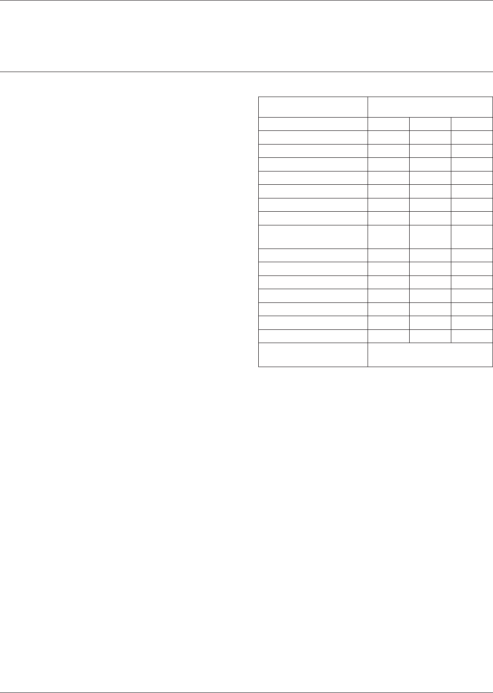
1.2.1 Establishing the Design Team The design team
can include but is not limited to the members who partici-
pate in at least the design activities identified in Table 1-1.
In this table, DfA/M stands for Design for Assembly/
Manufacturability, DfT for Design for Testability, DfR for
Design for Reliability.
The design team can consider the general design guidelines
and issues presented in the body of this document as a
methodology for achieving its reliability goals. Figure 1-1
illustrates the general design steps and process flow using
concurrent engineering. Figure 1-2 illustrates the interac-
tive nature of the design for reliability process.
1.2.2 Defining Reliability Requirements The basic reli-
ability requirements to be defined include:
• years of service
• acceptable failure rate(s)/probability(ies) as a function
of time
• repair/replacement/upgrade/service/maintenance/
warranty strategy
• life cycle environment(s)
• definition of acceptable performance
• criticality of function(s)
• available test equipment
1.2.3 Understanding the Product Life Cycle The life
cycle begins at the component level (including the printed
board) and continues through the assembly level; the life
cycle includes exposure to the following environments:
• assembly/process
• testing
• storage
• transportation
• operating
Table 1−1 The Design Team
Design/Engineering
Function Team Inprovement Area
Product (QFD) (DfA/M) (DfT) (DfR)
Circuit (QFD) (DfA/M) (DfT)
Printed board (DfA/M) (DfT) (DfR)
Thermal (QFD) (DfR)
EMC, EMI, ESD (QFD) (DfT) (DfR)
Mechanical (QFD) (DfA/M) (DfT) (DfR)
Software (QFD) (DfT)
Marketing (QFD)
Process/
manufacturing (QFD)
(DfA/M)
Test (QFD) (DfT) (DfR)
Package/component DfA/M) (DfT)
Field Service (QFD) (DfT)
Purchasing (DfA/M)
Material (QFD) (DfA/M) (DfT) (DfR)
Reliability (QFD) (DfA/M) (DfT) (DfR)
Regulations (QFD) (DfT)
Upper management (QFD) Conceptual Design
and Cultural Change
July 1996 IPC-D-279
1