IPC-D-279 EN.pdf - 第81页
convection. For most products using low power devices, strategic placement of a few ICs and careful venting in a housing or enclosure is adequate. For the products used in a friendly environment, such as the typical air …

heat exchanger, should be directed to cool the temperature-
sensitive parts first, and later be directed adjacent to the
higher power heat producing parts.
D-5.0 PRODUCT THERMAL DESIGN
The data for thermal resistance of junction-to-air, θ
ja
, and
of junction-to-case, θ
jc
should be available for all signifi-
cant power dissipaters.
Time and money can be saved with thermal simulation,
analysis and prediction programs on printed board and
PWA when those prediction programs are verified by ther-
mal analysis data taken with IR imagers or thermometers.
Thermally sensitive components should be identified.
These would include technologies with maximum rated
junction temperature T
j
≤85°C, such as high speed CMOS
and gallium arsenide (GaAs) with aluminum metallization
electromigration limitations or time-dependent-dielectric
breakdown mechanisms.
Where there are thermally sensitive components, heat dis-
sipaters should generally be ‘‘downstream’’ in the air flow;
under certain conditions of PWA geometry, component ori-
entation and relative component heights, turbulence may
result in ‘‘recirculation cells’’ conveying heat ‘‘upstream.’’
Where there are thermally massive heat dissipaters and
fans are required to cool the system, the design review
should include such items as component T
j
‘‘overshoot’’ on
fan turn-off.
Heat dissipaters should generally be ‘‘upstream’’ of tall
components to avoid recirculation cells.
Heat dissipater review should include those capacitors with
significant ripple current and ripple voltage; the data should
include Equivalent Series Resistance (ESR) vs. ripple cur-
rent, temperature, and frequency.
Where lower T
j
is required, should be considered the fol-
lowing avenues particularly applicable to SMT: thermal
vias, thermal solder joints, thermally conductive adhesives
from component to printed board, and power and ground
plans included in the thermal design. In addition, consider
the following moves: sensitive components ‘‘upstream’’ of
power dissipaters, power dissipaters further apart to reduce
power density, power dissipaters closer to cold wall (edge
of card if card clamps are used), and power dissipaters
‘‘upstream’’ of tall components.
To allow computation of the reliability of solder attach-
ments (see Appendix A), component lead flexural compli-
ance data should be available for the larger components or
for the components with stiffer leads; the critical package
dimensions and environmental temperature swings should
also be known.
Long, tall components such as connectors are ideally
placed parallel to the airflow. Placement of these compo-
nents perpendicular to the airflow results in the generation
of recirculation cells which reduce the heat transfer from
heat dissipaters or which increase heat transfer to heat sen-
sitive components.
Software for SM PWA and thermal design exist that allow
the designer to perform printed board thermal analysis
together with component junction temperature and reliabil-
ity prediction; some of the programs also address vibration,
fatigue, soldering, transmission line/parasitics aspects of
printed board design. Other programs perform thermal pre-
dictions on printed wiring boards, enclosures, heat sinks,
and plates, considering conduction within a printed board,
air temperature above components, and full convection and
radiation (steady-state and transient). Specialized programs
exist for computation of heat sink, heat fin and cold plate
performance, under steady state and transient conditions.
Powerful computer simulation programs run on engineer-
ing computers or PCs for airflow thermal analysis of elec-
tronic equipment cabinets or mixed fluid flows.
D-5.1 Component Level Cooling SM components are
low profile compared to through hole (TH) components
and are therefore more sensitive to the height of surround-
ing components and their airflow ‘‘shadowing’’ effects.
Also, the SM component has no airflow between the bot-
tom of the component and the printed board; the heat trans-
fer in this area is by conduction through the air.
Guidelines on placement of components based on two
dimensional airflow simulations and models do not apply
to typical SM PWAs. Under natural or low air flow forced
convection conditions, heat dissipaters should be ‘‘down-
stream’’ from thermally sensitive components. Taller pas-
sive, temperature-insensitive components should be
‘‘downstream’’ of heat dissipaters, and heat dissipaters
should not be in the airflow ‘‘shadow’’ (recirculation
region) of taller ‘‘upstream’’ components. Recirculation
regions result in a decrease in the heat transfer coefficient
of the heat dissipater and an increase in temperature of the
other component(s) sharing the heated recirculated airflow.
Under high flow forced convection conditions, recircula-
tion cells can form upstream of a taller, wider component
and reduce its heat transfer coefficient or unexpectedly
increase the temperature of upstream parts. It helps to turn
the long axis of the component parallel to the air flow, to
avoid stacking such components end to end perpendicular
to the air flow, and to increase the distance to upstream
parts. Low frequency oscillations in air flow and subse-
quent variations in component temperature may result
under some circumstances of parts orientation, heat dissi-
pation and air velocity.
D-5.2 Hot Parts (Thermal Considerations) Common
methods for controlling thermal rise of our electronic
assemblies is forced air, liquid cooling systems or natural
July 1996 IPC-D-279
69
convection. For most products using low power devices,
strategic placement of a few ICs and careful venting in a
housing or enclosure is adequate. For the products used in
a friendly environment, such as the typical air conditioned
office, one board assembly will survive indefinitely. But as
the complexity and component density increases, creative
thermal management techniques must be adopted.
Transferring heat from the component body of ICs and
power regulators usually requires some form of physical
contact to a mass of material attached to the device. Using
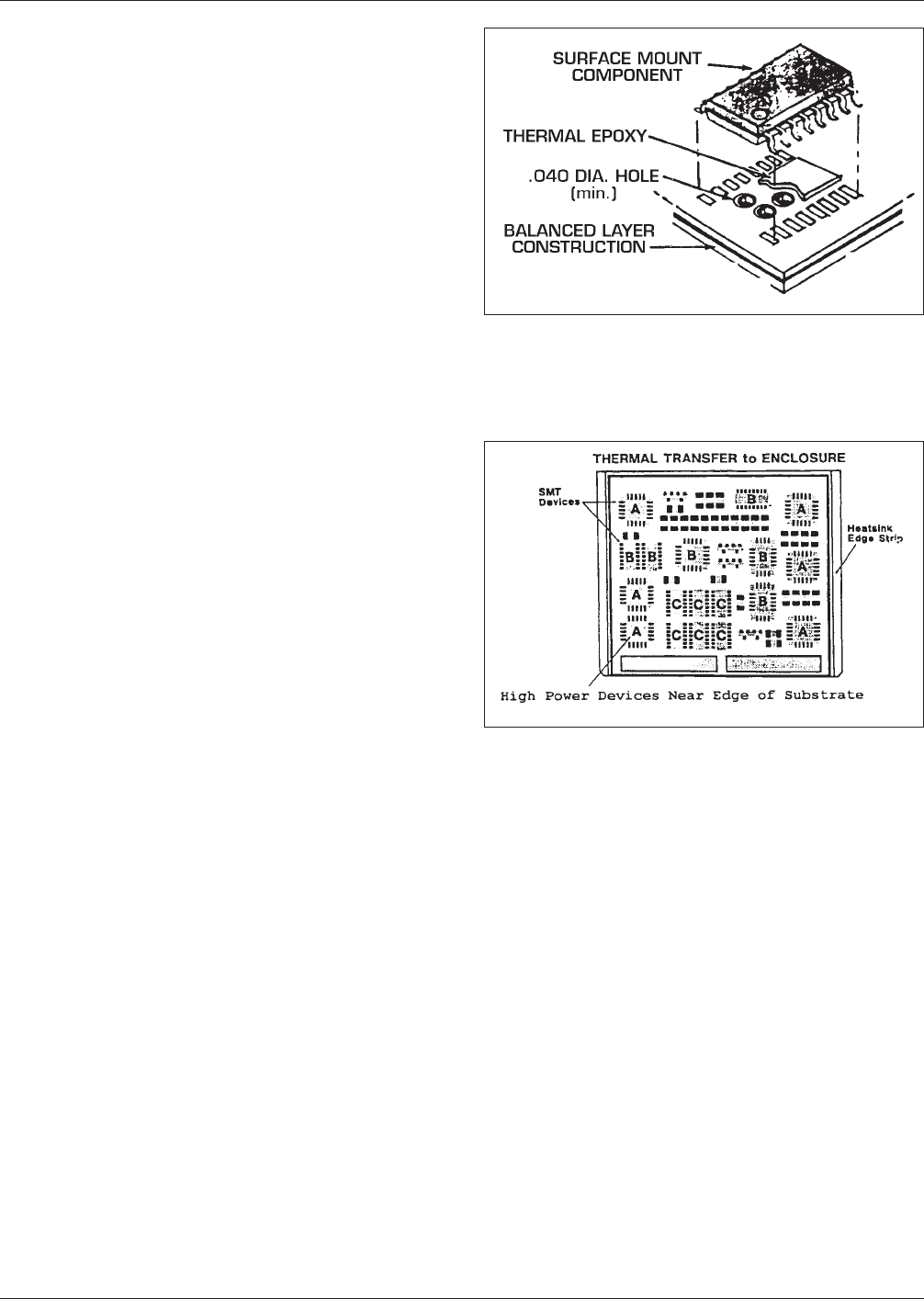
hardware or thermally conductive adhesives, as shown in
Figure D-1 is a common practice for thermal management.
The thermal rise can be distributed to a larger surface area,
thereby keeping the component within a recommended
operating temperature range. The efficiency of this dissipa-
tion and distribution is reliant on the area of the heatsink
mass and the loss expected through the interface media.
When attachment hardware is used, a thermal compound is
applied to prevent air, moisture and contaminants from
forming between surfaces. When epoxy attachment is nec-
essary, a thermally conductive material is chosen. The most
efficient thermal conductive epoxy usually contains an
electrically conductive filler. When maximum insulation is
also critical, the heat transfer efficiency from the compo-
nent to the heatsink will be reduced. Researchers are work-
ing on new compounds each year to further improve these
thermal transfer characteristics, and heat transfer tech-
niques for through hole devices are as varied as the engi-
neer’s imagination.
Care must be taken that the thermal planes do not cause
tensile loading of the solder joints.
Typically signal layers on a printed board board are etched
in
1
⁄
2
ounce or 1 ounce copper clad dielectric. But 2 and 3
ounce copper is also available for use on power and ground
layers. Of course, if the heat transfer is a mechanical
attachment to the chassis, the ground plane or planes would
provide a thermal conduit to transfer the heat from the
component’s body into the internal copper layer of this
substrate. When specifying the copper thickness on each
side of one dielectric layer, the layers and copper thickness
should be distributed evenly as the example in Figure D-1.
A non-symmetrical lamination may warp excessively dur-
ing reflow solder process.
The thermal rise expected from the components must be
determined, and if this collective temperature rise is
beyond the recommended operating temperature limits of
the device; a careful evaluation of the component grouping
is in order. Distribution of higher power devices on the
outer edge of the substrate panels will provide the neces-
sary correction to control and distribute thermal rise away
from the components. The more direct the thermal path is
away from these components the better; don’t locate high
power devices in the center of the substrate. Rather, place
them closer to the heat transfer edge leaving low power
devices in the center area. See figure D-2.
Figure D-3 describes techniques used to transfer thermal
rise of a SMT device through the outer dielectric layer of
the printed board to an internal ground plane of metal core.
Multilayer printed boards may have power and ground
planes internally layered and intermixed with signal layers.
This mass of copper planes can be an efficient thermal
conductor to transfer heat to the outer edge of the substrate
or the chassis.
IPC-279-D1
Figure D−1 Thermal Vias and Planes
IPC-279-B2
Figure D−2 Other Methods of Conductive Heat Transfer
IPC-D-279 July 1996
70
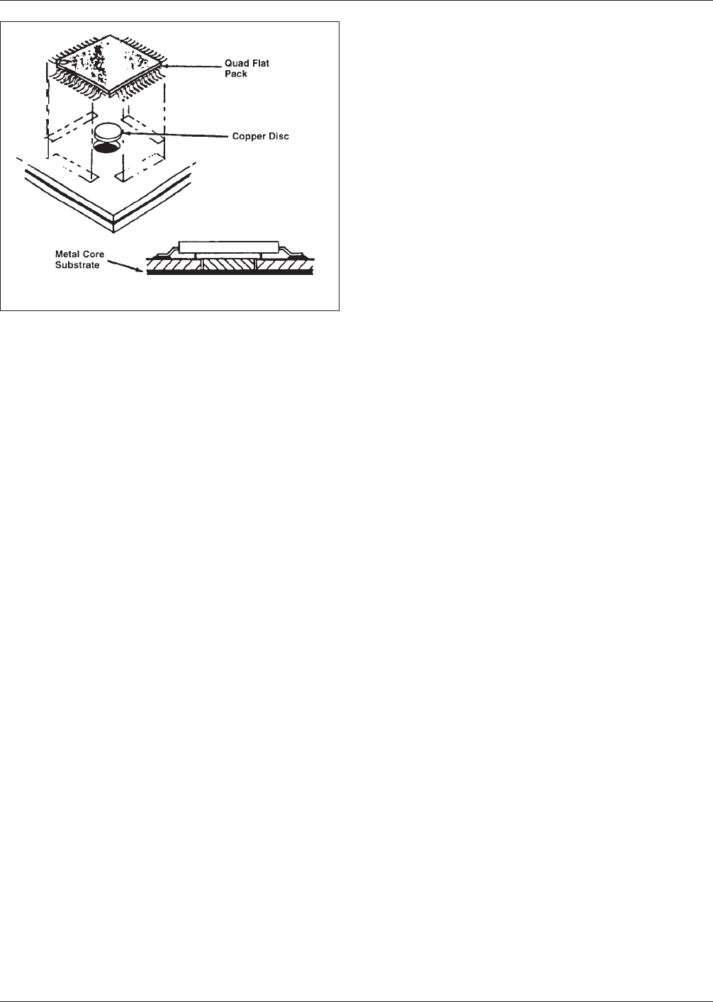
IPC-279-B3
Figure D−3 Use of Heat Slug
July 1996 IPC-D-279
71