IPC-D-279 EN.pdf - 第36页
the board T ype 2 —Components (mounted) on both sides of the board Class A —Through-hole component mounting only Class B —Surface mounted components only Class C —A mixture of through-hole and surface mounting The typica…

interactions. Failure to understand the links between board
manufacture, assembly processes and circuit design may
result in a choice of solder mask which will be costly to
reverse after introduction.
6.1.1 Solder Mask Selection Table 6-1 provides guide-
lines on solder mask selection.
6.1.2 Solder Mask Thickness Issues Regardless of the
type of solder mask used for surface mount applications,
the solder mask must be the correct thickness and consis-
tent. Solder mask plays an important role in forming a gas-
ket between the solder paste stencil and the printed board
to reduce the extrusion of paste and limiting smearing.
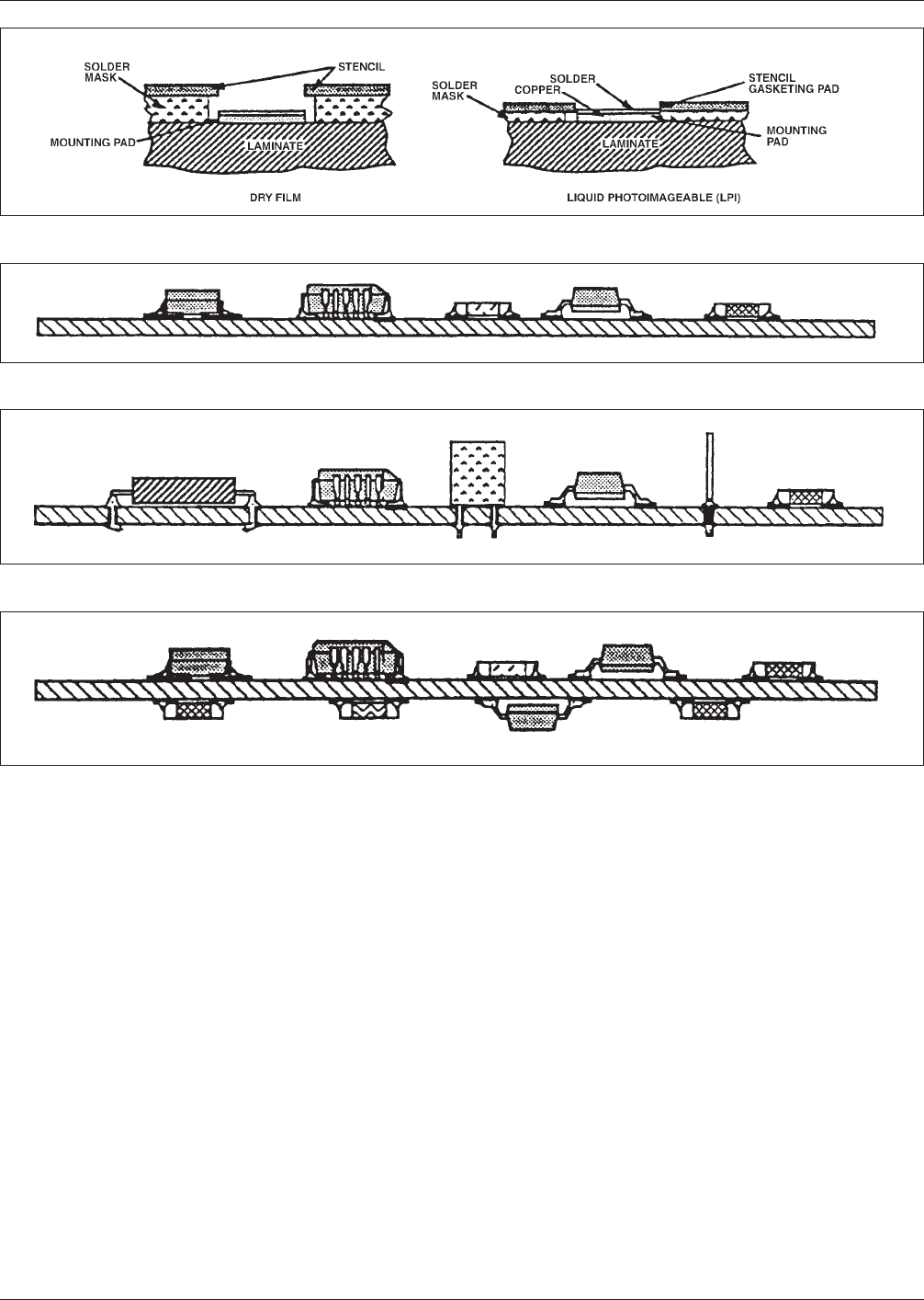
Typical dry film solder masks range from 75 to 100 µm
thick, leaving the mask higher than the surface mount pads
(see Figure 6-1). Thus, the stencil will rest on the solder
mask and leave a gap between the stencil and the pads
through which solder paste can flow. However, typical liq-
uid photoimageable masks range from 15 to 30 µm thick.
This makes the pad surfaces the highest points on the board
so that when the stencil is lowered, it will rest on the pads.
The stencil then gaskets the opening around the pads, pre-
venting the solder paste from getting under the stencil.
Excessively thick solder mask, particularly dry film over
traces under components with small clearance, can contrib-
ute to the formation of crevices which entrap flux. In the
case where the solder mask touches the bottom of the com-
ponent, if insufficient solder paste is used, it may result in
chip component drawbridging (tombstoning), insufficient
solder fillet or lack of solder joint. (See IPC-SM-782 and
IPC-D-275)
Solder joint reliability under temperature cycling or power
cycling conditions may be reduced if the solder mask
touches the bottom of the component or conformal coating
filling the printed board-component gap. (See IPC-SM-
785.)
6.2 Temporary Solder Mask and Tapes Temporary sol-
der mask and tapes are used to prevent solder and solvents
from causing problems during assembly processes. In SMT
the reflow techniques may expose the mask or tape to tem-
peratures which may cause thermal breakdown. This may
cause reversion of some materials into a sticky ‘‘goo’’ and
others may adhere tenaciously making them difficult to
remove. The cleaning of SM assemblies may also be more
aggressive than through-hole. It is necessary to verify that
the temporary mask selected is compatible with the assem-
bly processes.
6.3 Conformal Coatings The primary purpose of confor-
mal coatings is to provide environmental protection. Some
conformal coatings have been shown to significantly affect
the reliability of surface mount solder joints. Parylene
(trademark of Union Carbide, chemical name Polyparaxy-
lylene) and silicone conformal coating have been shown to
improve accelerated fatigue life of SM solder joints by
approximately a factor of two or three. However in thermal
shock, some silicone coatings have been reported to
decrease life in thermal shock.
7.0 ASSEMBLY PROCESSES AND DESIGN FOR MANU-
FACTURABILITY
While there are only a few processes used in fabricating an
assembly with SMT components, these processes directly
impact the formation of the solder joint that provides the
reliable attachment of the part to the substrate. It is essen-
tial that the designer of surface mount assemblies under-
stand the manufacturing processes involved, including their
impact on the reliability of the completed assembly. Design
for manufacturability requires that the designer have a clear
view of the impact and limitations of the fabrication steps.
IPC-CM-770, Printed Board Component Mounting,
includes the following classification scheme for surface
mount assemblies:
Type 1 —Components (mounted) on only one side of
Table 6−1 Solder Mask Guidelines
RECOMMENDED FOR THESE SM SOLDERING
PROCESSES
SOLDER MASK TYPE
APPLICATION
METHOD THICKNESS
TENTED
VIAS
STANDARD
PITCH
REFLOW
FINE
PITCH
REFLOW
WAVE
SOLDER
Liquid Screenprint 8-50 µm N* N N N
Dry Film Hot roll Lamination 60-100 µm Y Y N Y
Liquid Photoimageable Open Screen Coat
Curtain Coat
Roller Coat
Electrostatic Spray
15-30 µm N Y Y Y
Combination (liquid
photoimageable* dry
film cap layer)
Lamination 50-75 µm Y N Y
*The majority of via holes can be filled by this process but not tented.
IPC-D-279 July 1996
24
the board
Type 2 —Components (mounted) on both sides of the
board
Class A —Through-hole component mounting only
Class B —Surface mounted components only
Class C —A mixture of through-hole and surface
mounting
The typical assembly with surface mount components on
only one side of the substrate (Type 1B - Figure 7-1) is
assembled by one of the following sequences:
1. Apply adhesive, place SM components, cure adhe-
sive, wave solder, clean, test/repair.
or;
2. Apply solder paste, place SM components, reflow
solder paste, clean, test/repair.
If the assembly contains both surface mount and through-
hole components of a single-sided assembly (Type 1C Fig-
ure 7-2), it may be assembled using one of the following
sequences:
1. Apply adhesive, place SM components, cure adhe-
sive, wave solder, clean, insert through-hole compo-
nents and clinch, wave solder, clean, test/repair.
or;
2. Apply solder paste, place SM components, reflow
solder paste, clean, insert through-hole components
and clinch, wave solder, clean, test/repair.
When only surface mount components are mounted on
both sides of an assembly (Type 2B - Figure 7-3), there are
typically two assembly options:
1. Apply solder paste to side 2 (bottom), place SM
components, reflow solder paste, clean, invert board,
apply solder paste to side 1 (top), reflow solder paste,
clean, test/repair.
IPC-279-06
Figure 6−1 Impact of Solder Mask Thickness on Stenciling
IPC-279-07
Figure 7−1 Type 1B Assembly − All SMT Components
IPC-279-08
Figure 7−2 Type 1C Assembly − Mixed Technology Assembly
IPC-279-09
Figure 7−3 Type 2B − All SMT Components
July 1996 IPC-D-279
25
or;
2. Apply solder paste to side 2, dispense adhesive to
side 2, place SM components, cure/bake adhesive/
paste, invert board, apply solder paste to side 1, place
SM components, reflow solder paste, clean, test/
repair.
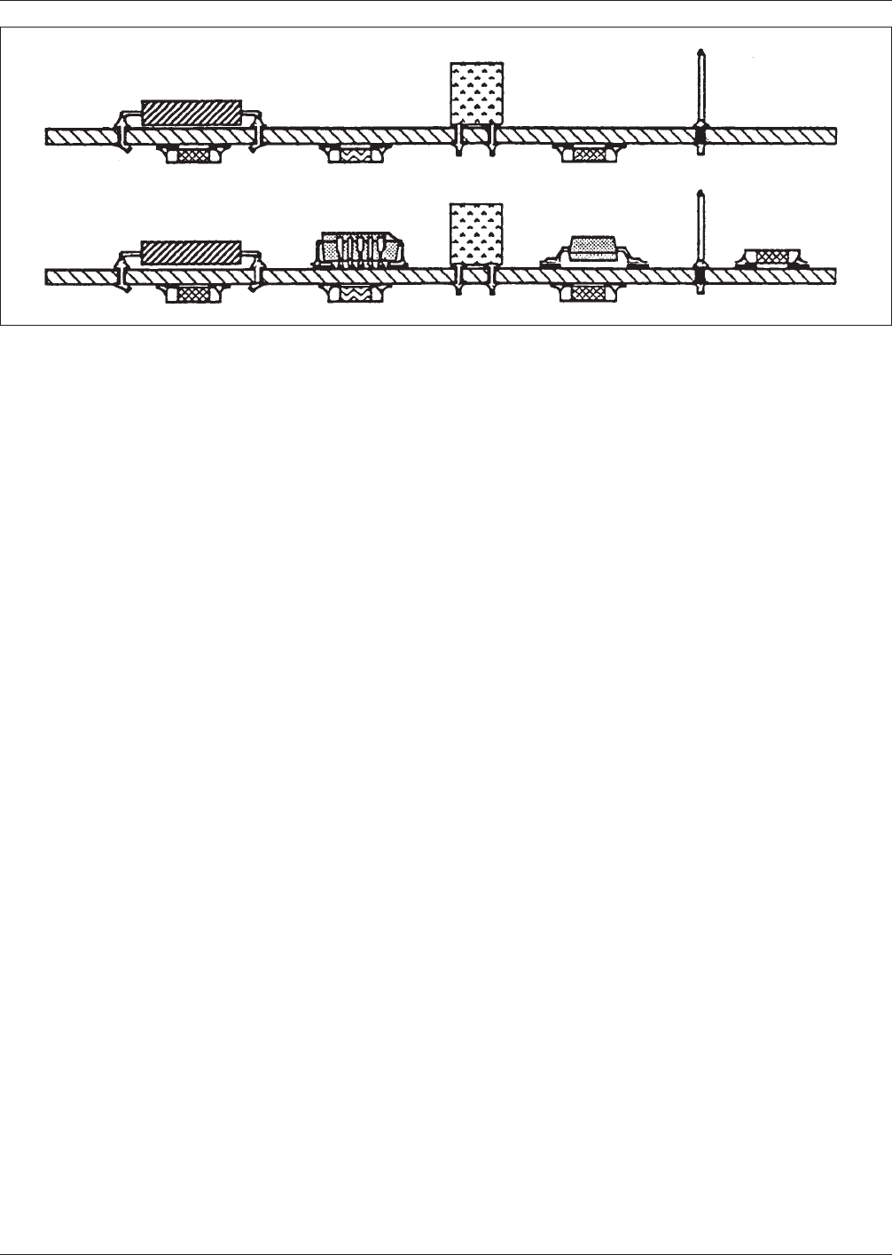
With mixed technology boards containing surface mounted
and through-hole components on more than one side of the
substrate (Type 2C - Figure 7-4), there are several typical
sequence possibilities:
1. For SM components on side 2 only: Apply adhesive
to side 2, place SM components, cure adhesive,
clean, invert board, insert through-hole components
and clinch, wave solder, clean test/repair.
or;
2. For SM components on both sides: Apply solder
paste to side 1, place SM components, reflow solder
paste, clean, invert board, apply adhesive to side 2,
place SM components, cure adhesive, invert board,
insert through-hole components and clinch, wave sol-
der, clean, test/repair.
3. For SM components on both sides: Apply adhesive to
side 2, place SM components, cure adhesive, apply
solder paste to side 1, place SM components, reflow
solder paste, clean, invert board, insert through-hole
components and clinch, wave solder, clean, test/
repair.
or;
4. For SM components on both sides: Apply solder
paste to side 1, place SM components, reflow solder
paste, clean, insert through-hole components and
clinch, apply adhesive to side 2, place SM compo-
nents, cure adhesive, invert board, wave solder,
clean, test/repair.
7.1 Solder Paste Application Solder paste may be
applied to a substrate either by syringe application or
screen/stencil printing. The first issue impacting reliability
at this stage is the alloy composition of the solder paste
being deposited. Solder comes in a variety of alloys includ-
ing combinations of tin, lead, silver, antimony, bismuth,
indium and cadmium. Each alloy has a distinct set of met-
allurgical properties and the selection should be based on
compatibility with the metals being joined (including
leaching and intermetallic formation), the service environ-
ment and the service/process temperatures. Reliability will
also be affected by the type of flux system used in the sol-
der paste; high reliability applications should be limited to
the use of R (rosin) or halide-free RMA (rosin-mildly acti-
vated) types.
Another contributor to reliability in this assembly operation
is the volume of solder paste deposited since it will dictate
the size of the solder joint. Careful consideration should be
given to parameters that will affect solder volume such as
stencil thickness and aperture sizes, squeegee/syringe pres-
sure, metal content of the solder paste and thickness of sol-
der coating on the printed board or substrate. See Appen-
dix M for details.
7.2 Adhesive Application Adhesive used to mount com-
ponents for subsequent wave soldering is typically applied
via a syringe dispensing method (either manual or auto-
matic). The volume of deposited adhesive should be
adequate to restrain the part in place but not impinge on
land areas or affect solderability and solder joint formation.
All adhesives should be tested for their tendency to form
voids that can entrap flux and affect long term reliability.
Adhesive voids may also be caused by curing the material
too rapidly. Adhesives may outgas even after complete cur-
ing.
7.3 Component Placement The placement of compo-
nents on the substrate may be accomplished either manu-
ally or by using a broad range of pick-and-place equip-
ment. Accurate positioning of components to their
IPC-279-10
Figure 7−4 Type 2C − Mixed Technology
IPC-D-279 July 1996
26