IPC-D-279 EN.pdf - 第29页
T able 4−1 Advantages and Disadvantages of V arious T ypes of Substrates TYPE MAJOR ADV ANT AGES MAJOR DISADV ANT AGES COMMENTS ORGANIC BASE SUBSTRA TE Epoxy fiberglass Substrate size, weight; reworkable; dielectric prope…

For the assembly to function properly, the electrical,
mechanical, and thermal requirements of each material
used in the substrate must be considered for the operating
conditions and use environments.
Table 4-1 provides guidance in the material choices. See
IPC-D-275 for other material discussions.
4.3 Moisture and its Effects on Polymer Substrates
Polymers commonly used in SMT printed boards absorb
and adsorb water when exposed to moist atmospheres (high
relative humidity) for durations ranging from several days
to several weeks; the equilibration time depends upon the
thickness of the laminates and the geometry of the conduc-
tor pattern. The relative permittivity of water is 80 and that
of common substrates ranges from 3 to 5; the absorption of
1-3% by weight of water can significantly (but reversibly)
increase the dielectric constant between conductors and
hence the capacitive coupling between conductors, over
time. The absorption and adsorption of water also
decreases the insulation resistance between conductors at
the surface (SIR). Together with ionizable contaminants
and DC bias, condensed moisture can lead to electro-
chemical corrosion and dendrites on the surface of the sub-
strates; conductive anodic filament (CAF) formation at the
glass fiber-resin interface; and electrochemical corrosion
and dendrites at delaminations and voids such as occur
between conductors on inner layers and between barrels of
PTVs and PTHs. Moisture effects are more significant in
SM printed boards because the spaces between conductors
and the interbarrel distances are much less than the corre-
sponding dimensions in through hole printed boards; in
addition, solder masks may not be easily applied between
land patterns in the fine and extra fine pitch SM patterns.
See Appendix C for DfR information on SIR. See also
IPC-TR-476.
Some materials with higher glass transition temperatures
(T
g
) such as bismaleimides and polyimides, appear to
absorb more water than the lower T
g
materials, such as the
epoxies. Drying of the higher T
g
materials (as well as
thicker buildups of the epoxy systems) prior to SM reflow
exposure or rework/repair is recommended to minimize
delamination or separation, for instance, of the conductor
from the resin or the glass fiber from the resin.
The laminate surface is porous when treated by etching to
enhance adhesion of conductors; this surface porosity can
retain hydrolyzable and ionizable contaminants and water,
as well as hydrophilic materials such as polyglycols which
are used in the formulation of some water soluble SM sol-
der pastes. Solder mask and conformal coating materials
cover and seal the porous surface and help to retain SIR
values and reduce the risk of corrosion.
Common solder masks (and conformal coatings) are per-
meable to water vapor; the presence of water soluble con-
taminants between solder mask or conformal coating and
the underlying surface can result in vesication or mealing
and in electrochemical corrosion/migration.
Chemisorption of water into polymers appears to reduce
the T
g
slightly, reduces the adhesion of the polymer to
other materials and reduces the strength of the polymer.
See also the bibliography of IPC-SM-786.
4.4 Coefficient of Thermal Expansion (CTE) of Polymer
Systems
Polymer systems expand with increasing tem-
perature, demonstrating a glassy phase response below T
g
with a CTE or α
1
and a rubbery phase response above T
g
with a much higher α
2
, typically 3 times α
1
. The transition
from glassy phase to rubbery phase is gradual, but for most
polymer substrates may be characterized by T
g
, the glass
transition temperature.
Glass fiber reinforced substrates exhibit significantly differ-
ent CTE in the z (out of plane) axis compared to the CTE
in the x and y axes; for example, below its T
g
, Quartz/
Bismaleimide material with 35% resin by weight exhibits a
CTE(x-y) of 6 ppm/°C and a CTE(z) of 41. Woven glass
fiber reinforcement exhibits an additional difference
between x and y axes on the order of 1-5 ppm/°C; this dif-
ference may be significant where the CTE of a large SM
component package is to be matched to the CTE of the
substrate to enhance cyclic life of the solder attachments.
The CTE(z) is particularly significant in determining the
cyclic life of PTH and PTVs in SM PWAs because the
aspect ratio (ratio of substrate thickness to finished hole
diameter) is generally much larger than the corresponding
aspect ratio achieved in printed boards manufactured for
through hole technologies. Higher CTE(z) values result in
higher cyclic tensile stress in the barrel of the PTH or PTV
during temperature excursion during SM reflow, or SM
component removal/rework/repair as well as during printed
board fabrication, solder dipping, hot air leveling, or wave
solder. See IPC-TR-579 and IPC-SM-782.
The thermal cycle reliability, vibration robustness, and the
thermal management of high performance Surface Mount
(SM) products are heavily dependent upon the constraining
core such as copper-molybdenum-copper (CMC), copper-
Invar-copper (CIC) and molybdenum-graphite-
molybdenum (MGM) composite material systems.
The ratios of the various materials in those composite sys-
tems can be adjusted to tailor the effective CTE to the opti-
mum value. The tradeoffs include weight and cost. See
IPC-MC-324.
4.5 Constraining Cores in Substrates A constraining
core is an internal supporting plane in a packaging and
interconnecting structure, used to alter the coefficient of
thermal expansion of printed boards.
July 1996 IPC-D-279
17
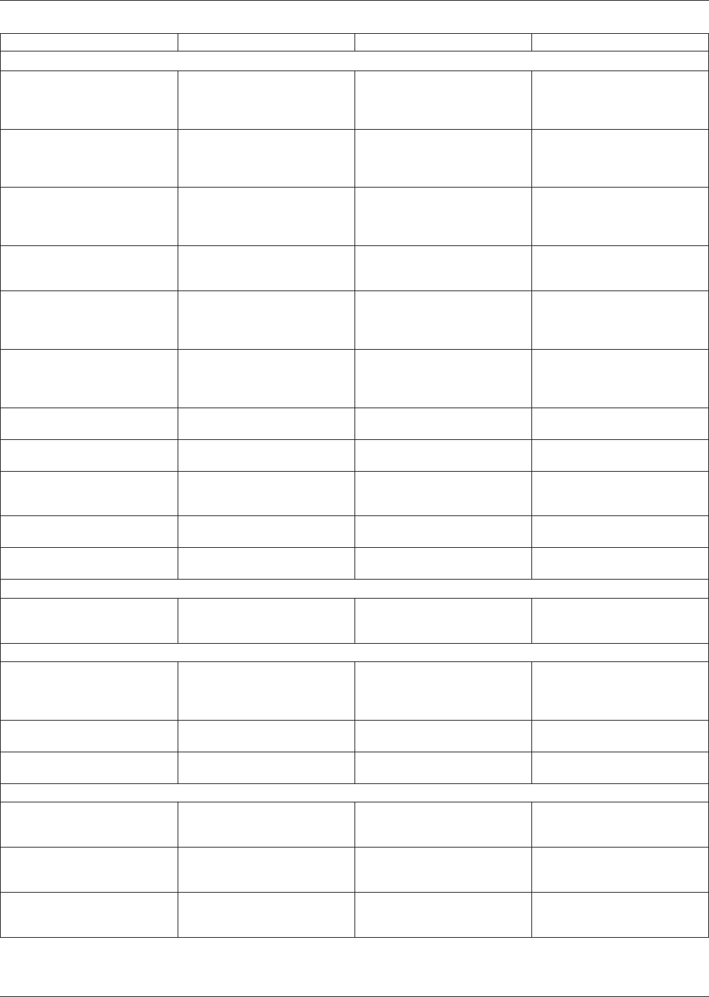
Table 4−1 Advantages and Disadvantages of Various Types of Substrates
TYPE MAJOR ADVANTAGES MAJOR DISADVANTAGES COMMENTS
ORGANIC BASE SUBSTRATE
Epoxy fiberglass Substrate size, weight; reworkable;
dielectric properties; conventional
board processing, availability,
cost/performance value.
Thermal conductivity x, y, and z axis CTE a concern for
high density applications.
Polyimide fiberglass Same as epoxy fiberglass plus
high temperature z axis CTE;
substrate size; weight; reworkable,
dielectric properties.
Thermal conductivity; moisture
absorption.
Same as epoxy fiberglass; x, y,
and z axis CTE a concern for high
density applications.
Epoxy aramid fiber Same as epoxy fiberglass; x-y axis
CTE; substrate size; lightest
weight; reworkable; dieletric
properties.
Thermal conductivity; resin
microcracking; z axis CTE; water
absorption; cost; resin adherence.
Volume fraction of fiber can be
controlled to tailor x-y CTE. Resin
selection critical to reducing resin
microcracks.
Polyimide aramid fiber Same as epoxy aramid fiber; z
axis CTE; substrate size; weight;
reworkable; dielecric properties.
Thermal conductivity; resin
microcracking; water absorption;
cost; resin adherence.
Same as epoxy aramid fiber.
Polyimide quartz (fused silica) Same as polyimide aramid fiber; x,
y, z axis CTE; substrate size;
weight; reworkable; dielectric
properties.
Thermal conductivity; drilling;
availability; cost; low resin content
required.
Volume fraction of fiber can be
controlled to tailor x-y CTE. Drill
wearout higher than with
fiberglass.
Fiberglass/Teflon laminates Dielectric constant; high
temperature stability; thermal
conductivity; x and y axis CTE.
Same as epoxy fiberglass; low
temperature stability; thermal
conductivity; x and y axis CTE;
difficult processing.
Suitable for high speed logic and
high frequency applications. Same
as epoxy fiberglass.
Flexible dielectric Lightweight; minimal concert to
CTE; configuration flexibility.
Size Rigid-flexible boards offer tradeoff
compromises.
Thermoplastic 3-D configurations; low
high-volume cost.
High injection molding setup costs;
additive processing.
Very limited applications.
Bismaleimide/triazine glass Improved dielectric properties;
multiple thermal shock; minimum
cost penalty for upgrade.
Thermal conductivity; x, y, and z
axis CTE.
Applicable to MCM-L technology.
Composite CEM-1 and CEM-3 Punchable at room temperature;
cost; stiff enough for SMD.
x and y axis CTE; thermal
conductivity.
Substrate of choice for consumer
products with SMDs.
Paper-based phenolic Punchable with heat; lowest cost. Single-sided only; stiffness;
availability; x and y axis CTE.
Majority of world market is
paper-based.
NONORGANIC BASE
Alumina (ceramic) CTE; thermal conductivity;
conventional thick film or thin film
processing; integrated resistors.
Substrate size; rework limitations;
weight; constant; brittle; dielectric
constant.
Most widely used for hybrid circuit
technology.
SUPPORTING PLANE
Printed board bonded to plane
support (metal or nonmetal)
Substrate size; reworkability;
dielectric properties; conventional
board processing x-y axis CTE;
stiffness; shielding; cooling.
Weight The thickness/CTE of the metal
core can be varied along with the
board thickness, to tailor the
overall CTE of the composite.
Sequential processed board with
supporting plane core
Same as board bonded to
supporting plane.
Weight Same as board bonded to
supporting plane.
Discrete wire High speed interconnections; good
thermal and electrical features.
Licensed process; requires special
equipment; cost; availability.
Same as board bonded to low
expansion metal support plane.
CONSTRAINING CORE
Printed board bonded with
constraining metal core
x and y axis CTE; uses FR-4 or
polyimide/glass materials.
Weight; internal layer registration;
delamination; via hole cracking, z
axis CTE.
Can be used as power/ground
planes.
Printed board bonded to low
expansion graphite fiber core
Same as board bonded to low
expansion metal cores; stiffness,
thermal conductivity; low weight.
Cost; microcracking; z axis CTE. The thickness of the graphite and
board can be varied to tailor the
overall CTE of the composite.
Compliant layer structures Substrate size; dielectric
properties; x-y axis CTE.
z axis CTE; thermal conductivity. Compliant layer absorbs difference
in CTE between ceramic package
and substrate.
IPC-D-279 July 1996
18

As with printed boards with supporting planes, one or more
supporting metallic or non-metallic planes can serve as a
stiffener, heatsink, and/or CTE constraint in constraining
core printed boards.
The results of ‘‘accelerated’’ life tests which incorporate
temperatures which approach or exceed the T
g
of the sub-
strate should not be extrapolated to predict service life;
these tests may be used to discriminate between alterna-
tives.
4.5.1 Printed Board Stiffness and Damping Con-
strained core systems with skins of high modulus material
form boards which in comparison with standard base mate-
rials are stiffer and have higher damping frequencies. These
characteristics may be beneficial, depending upon the envi-
ronmental vibration and noise spectrum.
4.6 Flexible Printed Board with Metal Support Plane
Another arrangement for a printed board with leadless
components involves conventional fine-line polyimide flex-
ible printed wiring. These assemblies can be constructed in
multilayer form while retaining the low-modulus feature
that reduces residual strain at the solder joints. Further-
more, lasers can drill very fine holes in the thin, printed
wiring laminate. These holes can be plated-through or
filled with solid copper as required.
To retain inherent flexibility while dissipating heat from the
solder joint, cutouts in the flexible circuit accommodate
pillars from the metal heatsink support plane. Although this
appears to be heavy and cumbersome, if the heatsink base-
plates are made from thin sheets of aluminum, the result-
ing density of the combined circuit/heatsink assembly
might actually be less than other constructions.
4.7 Discrete Wire Structures with Metal Support
Plane
Discrete wire printed boards have been developed
specifically for use with surface mounted components.
These structures are usually built with a low-expansion
metal support plane that also offers good heat dissipation.
The interconnections are made by discrete 0.06 mm diam-
eter insulated copper wires precisely placed on a 0.03 mm
grid by numerically-controlled machines. This geometry
results in a low-profile interconnection pattern with excel-
lent high-speed electrical characteristics and a density nor-
mally associated with thick film technology.
The wiring is encapsulated in a compliant resin to absorb
local stresses and dampen vibration. Electrical access to the
conductors is by 0.25 mm diameter copper vias. The small
via size can be accommodated in the component attach-
ment land, thus eliminating the need for fanout patterns
when using components with terminals on centers as close
as 0.6 mm, and allowing very-high packaging densities.
The high level of water absorbed into polyimide tape auto-
mated bonding (TAB) substrate materials during exposure
to high ambient moisture levels has been observed to result
in conductor corrosion and delamination.
4.8 Outgassing of Polymer Substrates See also the dis-
cussion of solder mask and coatings in Appendix N, and
section 6. The printed board may contribute emissions of
cleaning solvent, polyglycols, and lighter fractions of flux
vehicles in addition to the emission from the solder mask
and conformal coating of the printed board and of the com-
ponent encapsulation materials.
4.9 Assembly Process Effects on Polymer Substrates
See also the discussion of rework and repair in section 7.6
and Appendix E.
In addition, fluxes for wave soldering and for water soluble
solder pastes can contain high boiling point hydrophilic or
hygroscopic solvents such as the polyglycols. These sol-
vents can penetrate the resin-glass fiber interface and con-
tribute to conductive anodic filament (CAF) formation. See
Appendix C for DfR information. See also IPC-TR-476.
4.10 Printed Board Solderability The land patterns in
IPC-SM-782, particularly for those intended for fine pitch
and extra fine pitch components, clearly demonstrate the
very small areas available for affecting the solder joint in
SM technology. A solderability defect with an area of 125
µm by 250 µm which might be discounted on a through
hole board may constitute the single land which is non-
solderable on a SM board and render that SM PWA non-
functional; worse, the component lead may contact the land
and mechanically affect an electrical contact which
becomes intermittent in service and the product is a NTF or
No Trouble Found at the repair center.
Although solder dipping and hot air solder leveling
(HASL) are said to constitute ‘‘proof’’ that the land is sol-
derable, these processes do not characterize solderability of
the land at the critical time which is just before the solder
paste is applied and the components are placed. Printed
board land solderability is degraded by oxides or chlorides
of tin and lead oxides or chlorides of tin-lead phases;
oxides of tin-copper intermetallic compounds; and organic
films such as residues from fluxing oils, finger prints or
solder mask. These oxides, chlorides and organic films can
form after the HASL process. See also IPC-PE-740 and
IPC-S-816. Quantification of the solderability of the SM
printed board is difficult but is addressed in ANSI/J-STD-
003; an earlier specification is IPC-S-805.
4.11 Design for Reliability of Plated-Through-Hole Vias
(PTVs)
The material in Appendix B gives a detailed treat-
ment of DfR for PTVs.
5.0 GENERAL COMPONENT SELECTION CONSIDER-
ATIONS
1. During circuit design and verification, primary
impact on manufacturing and reliability lies in the
July 1996 IPC-D-279
19