IPC-D-279 EN.pdf - 第109页
T able G−2 Properties of Printed Circuit Laminates 1 Thermal Mechanical Material Conductivity W/M-K CTE X, Y Dir . ppm/°C CTE Z. Dir ppm/ Max. Use T emperature °C Glass T ransition T emp. °C T ensile Strength MP a Y ield…

Insulator/Substrate
Material/System
CTE
lower value upper
Conductor Material/System
Alloy 42 4.4
Alluminum (40% Silicon) 13.5
Aluminum, T6061 23.6
Boron Aluminum (20%) 12.7
Copper, CDA 101 17.6
Copper/Invar/Copper
20/60/20 Thick
5.7 5.8
Copper/Molybdenum/
copper 20/60/20 Thick
7
Gold 14
Graphite/Aluminum 4 6
Invar 36 1.6
Invar 42 4.5
Kovar 5
Lead 29
Lead (95%) Tin Solder 28
Lead-Tin solder 60/40 23 25
Molybdenum 4.9
Ni-clad Molybdenum 5.2 6.0
Silver 19
Tungsten/Copper (90/10) 6.0 6.5
Tungsten 4
July 1996 IPC-D-279
97
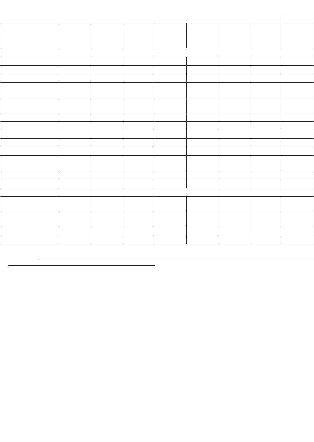
Table G−2 Properties of Printed Circuit Laminates
1
Thermal Mechanical
Material
Conductivity
W/M-K
CTE
X, Y Dir.
ppm/°C
CTE
Z. Dir
ppm/
Max. Use
Temperature
°C
Glass
Transition
Temp.
°C
Tensile
Strength
MPa
Yield
Strength M
Pa
Elongation
%
Polymer Composites:
Polyimide Glass 0.35 12-16 40-60 215-280 250-260 345 —
Epoxy Glass
(a)
0.16-0.2 14-18 180 130-160 125-135 276 —
Modified Epoxy
(b)
- 14-16 — — 140-150 — —
PTFE
(e)
Glass,
Non-Woven
0.1-0.26 20 — 230-260 — — —
PTFE
(e)
Glass,
Woven
419-837 10-25 — 248 — 38-52 —
Epoxy Aramid 0.12 6-8 66 — 125 68-103 — —
Epoxy Quartz - 6-13 62 — 125 — —
Polyimide Aramid 0.28 5-8 83 — 250 — —
Polyimide Quartz 0.35 6-12 35 — 188-250 207 —
Epoxy - Cordierite 0.9-1.3 3.3-3.8 ——————
Modified Epoxy
Aramid
— 5.5-5.6 100 — 137 — —
PTFE
(e)
Quartz — 7.5-9.4 88 — 19
(d)
——
Polyimide 4.3-11.8 45-50 — 260-315 — — — 6-7
Metal Composites:
Cu/lnvar/Cu (20/60/
20)
15-18
(c)
5.3-5.5 16 — N/A 310-414 170-270 36
Cu/lnvar/Cu (12.5/75/
12.5)
14
(c)
4.4 — — N/A 380-480 240-340
Cu/Mo/Cu 90-174 2.6 — — N/A — —
Ni/Mo/Ni 129.8
(c)
5.2-6 5.2-6 — N/A 621 552 50
(a) FR-4, G-10 (b) Polyfunctional FR-4 (c) Z-direction (d) Polymorphic p (e) PTFE=Polytetrafluoroethylene
(1) See material in Technology Assessment of Laminates, IPC-TA-720; Materials for High Density Electronic Packaging and Interconnection; ‘‘Thermal Expansion
Properties’’ chapter of Electronic Materials Handbook, Volume 1, Packaging. These values are most useful when accompanied by an indication of the ratio of
reinforcement to matrix. The chemical combination of epoxy and polyimide yields bismaleimide.
IPC-D-279 July 1996
98

Appendix H
Electrostatic Discharge
H-1.0 INTRODUCTION
H-1.1 ESD Susceptibility and Damage Prevention
All
electronic components containing thin conducting or insu-
lating films are susceptible to electrostatic discharge (ESD)
damage. These components include those fabricated in
high speed technologies (MOS, Bipolar, GaAs), thin film
technologies (resistors, integrated circuits, magnetic heads,
MOS capacitors), and in future, wafer scale integration and
multichip modules.
The best place for ESD protective circuitry is inside the
component package.
H-1.2 Current Limiting (ESD) SM resistors/SM inductors
which are unencapsulated and networks which are delami-
nated between pins or across the inductive or resistive ele-
ment should not be counted upon to limit current during
ESD events. The dielectric strength of air at sea level is
~1200 volts/mm. A 0.5 mm air gap or space can support
only ~600 volts before breaking by sparking across the
small air gap space between electrodes at the edge of the
dielectric. SM capacitors which are un-encapsulated will
also break down; some MOS capacitors are protected by
preferential sparking across the small air gap space
between electrodes at the edge of the dielectric. The dielec-
tric strength of most moulding compounds is ~20,000
volts/mm.
H-1.3 Susceptible Parts and Workarounds If parts sus-
ceptible to ESD, EOS, high speed transients or latchup
cannot be avoided, consult resources such as Circuits,
Interconnections, and Packaging for VLSI, Decoupling and
Layout of Digital Printed Circuits, or Protection of Elec-
tronic Circuits from Over-voltages. Electrical Assessment
of GaAs Digital Microcircuits covers some GaAs ESD
issues. High currents resulting from ESD have some pre-
dictable characteristics (1989-1991 National Institute of
Science and Technology publications).
H-1.4 Assembly Process and Handling Packaging and
handling of parts with ESD sensitivity must be done prop-
erly at all times, from their fabrication by the supplier
through installation of the finished assemblies in the end
product. In particular, they must be delivered and stored on
static-free tape and reel (T/R), and shielded from outside
sources of ESD. The problem is that suppliers ignorant of
any danger to their product will use the cheapest packag-
ing materials they can find. These packing materials may
be ineffective at best, and sources of ESD generation on
production lines at worst. Electrostatic Discharge Control,
Handbook of ESD Control: The Comprehensive and Sen-
sible Approach, ESD Program Management, and ESD from
A to Z are some books addressing the assembly, handling,
and transportation aspects of ESD control in the processes.
Some convective reflow ovens are said to result in ESD
levels of 200V on the PWA in the hot, dry, fast moving air
environment. Some de-reeling environment (tape and reel
material, dry air, rapid de-reeling) are said to result in ESD
levels in excess of 10 kV.
H-2.0 ESD DESIGN AND CHECKLIST
H-2.1 Hardware Design
In this appendix is an abbrevi-
ated design checklist addressing hardware ESD issues.
H-2.2 Assembly Process and Handling Electrostatic
Discharge types:
Air Discharge is tricky; at 20 kV, arc may jump to shield
but at 2 kV, arc may jump to connector pin. You cannot
‘‘accelerate’’ ESD air discharges by increasing voltage.
You cannot simply verify ESD susceptibility of the assem-
bly at the high end and assume that the low end is taken
care of.
Rule of thumb
20kV jumps 20 mm in air
2 kV jumps 2 mm in air
Concern for
(conductive injection)
(secondary arc injection)
Contact discharge is more repeatable but less frequent in
real life—except for cables with low electrostatic voltage.
H-2.2.1 Firmware/Software ESD Design Guidelines
(Possibly least expensive to implement)
Refresh, at regular intervals, the following
Interrupts
Stop bit level for serial data output
Latch and port output status
Control and Selection Inputs
Check and Restore
Program flow checkpoints
Hardware timer for fail-safe watchdog or system reset
Redundant data storage and comparison
Value/Range of data in index registers
Value/Range of data in inputs
Frame error check
Parity
Checksum
Echoing
Periodic check for ESD induced ‘‘sleep’’ state
Verify critical inputs such as interrupts and resets
Debounce software
July 1996 IPC-D-279
99