IPC-D-279 EN.pdf - 第46页
and all leaded solder joints, show localized damage con- centrations with the damage shown in Figure A-1 preced- ing an advancing macro-crack. The solder joints frequently connect materials of highly disparate properties…

Appendix A
Design for Reliability (DfR) of Solder Attachments
A-1.0 SURFACE MOUNT SOLDER ATTACHMENT
RELIABILITY
The fatigue behavior of surface mount solder joints has
been investigated experimentally in numerous studies. The
results of the studies that were carried out in a manner to
assure the same damage mechanism as the mechanism
operative in typical electronic products have yielded a
mathematical solder fatigue model. This model has been
expanded and augmented to its current form, presented in
this section, as additional test results became available.
The model is for uncoated solder attachments. The com-
plexity and vast differences in conformal coatings make it
impossible to develop a generic model that considers all
the variables. Products with conformal coatings should be
evaluated using test vehicles having the same coating and
test vehicles without the coating in order to assess the
impact of the coating on reliability.
A-2.0 DAMAGE MECHANISMS AND FAILURE
The reliability of electronic assemblies depends on the reli-
ability of their individual elements and the reliability of the
mechanical thermal, and electrical interfaces (or attach-
ments) between these elements. One of these interface
types, surface mount solder attachment, is unique since the
solder joints not only provide the electrical interconnec-
tions, but are also the sole mechanical attachment of the
electronic components to the printed board and often serve
critical heat transfer functions as well.
A solder joint in isolation is neither reliable nor unreliable;
it becomes so only in the context of the electronic compo-
nents that are connected via the solder joints to the printed
board. The characteristics of these three elements - compo-
nent, substrate, and solder joint - together with the use
conditions, the design life, and the acceptable failure prob-
ability for the electronic assembly determine the reliability
of the surface mount solder attachment.
A-2.1 Solder Joints and Attachment Types
Solder joints are anything but a homogeneous structure. A
solder joint consists of a number of quite different materi-
als, many of which are only superficially characterized. A
solder joint consists of:
(1) the base metal at the printed board
(2) one or more intermetallic compounds (IMC)—
solid solutions—of a solder constituent—
typically tin (Sn)—with the printed board base
metal
(3) a layer from which the solder constituent form-
ing the printed board-side IMC(s) has been
depleted
(4) the solder grain structure, consisting of at least
two phases containing different proportions of
the solder constituents as well as any deliberate
or inadvertent contaminations
(5) a layer from which the solder constituent form-
ing the component-side IMC(s) has been
depleted
(6) one or more IMC layers of a solder constituent
with the component base metal, and
(7) the base metal at the component.
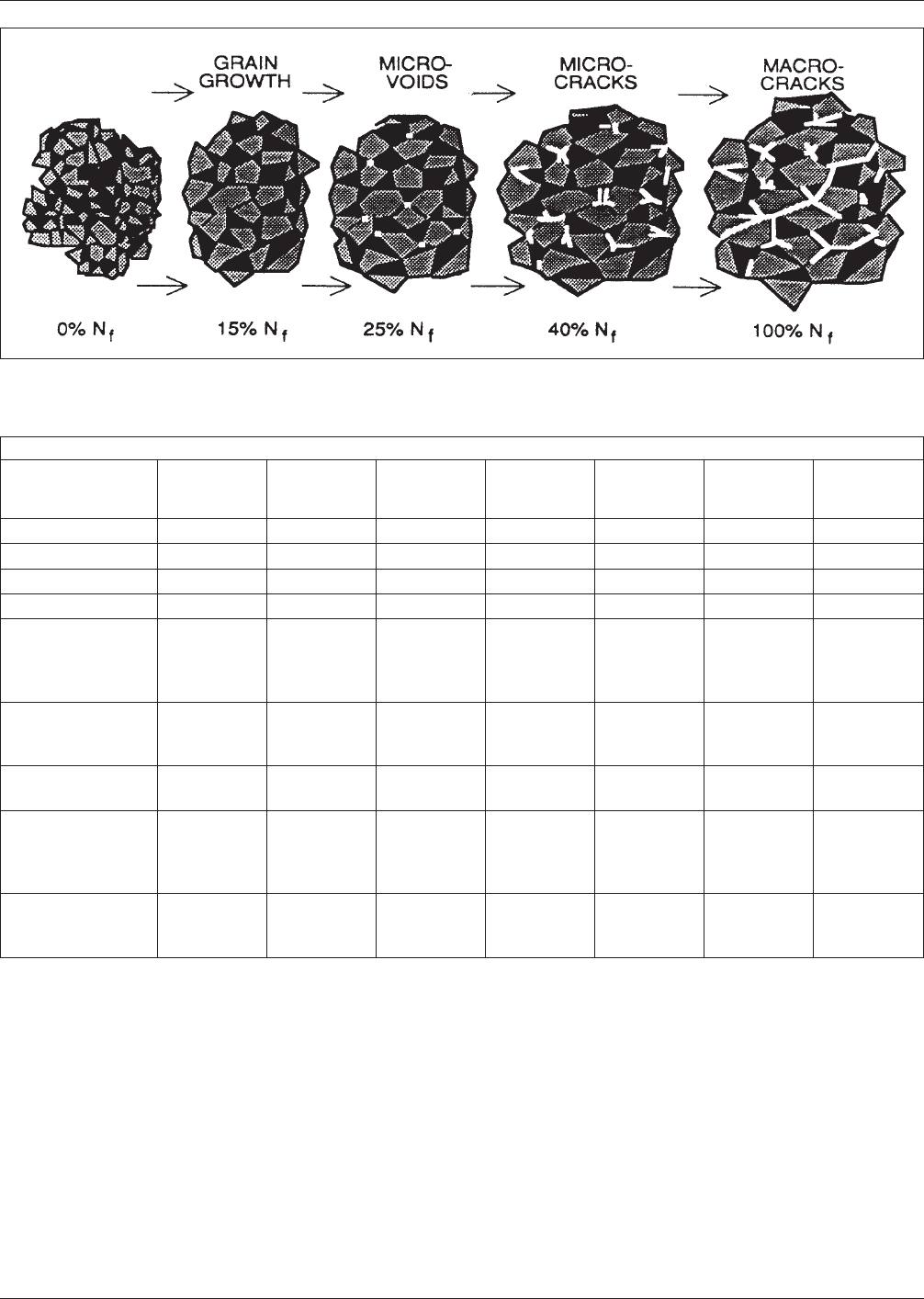
The grain structure of solder is inherently unstable. The
grains will grow in size over time as the grain structure
reduces the internal energy of a fine-grained structure. This
grain growth process is enhanced by elevated temperatures
as well as strain energy input during cyclic loading. The
grain growth process is thus an indication of the accumu-
lating fatigue damage. At the grain boundaries contami-
nants like lead oxides are concentrated; as the grains grow
these contaminants are further concentrated at the grain
boundaries, weakening these boundaries. After the con-
sumption of ~25% of the fatigue life micro-voids can be
found at the grain boundary intersections; these micro-
voids grow into micro-cracks after ~40% of the fatigue
life; these micro-cracks grow and coalesce into macro-
cracks leading to total fracture as is schematically shown in
Figure A-1.
Surface mount solder attachments exist in a wide variety of
designs. The major categories are leadless and leaded sol-
der attachments. Among the leadless solder joints a differ-
entiation has to be made between those without fillets, e.g.,
Flip-Chip C4 (Controlled Collapse Chip Connection) sol-
der joints, BGAs with C5 (Controlled Collapse Chip Car-
rier Connection) solder attachments, BGAs with high-
temperature solder (e.g., 10Sn/90Pb) balls, and CGAs with
high-temperature solder columns; and solder joints with
fillets, e.g., chip components, Metal Electrode Face compo-
nents (MELFs), and castellated leadless chip carriers. The
leaded solder attachments differ primarily in terms of their
compliancy and can be roughly categorized into compo-
nents with super-compliant leads {K
D
<~9 N/mm}, compli-
ant leads (~9 N/mm<K
D
<~90 N/mm), and non-compliant
leads {(K
D
>~90 N/mm}.
The different surface mount solder attachment types can
have significantly different failure modes. Solder joints
with essentially uniform load distributions, e.g., Flip-Chip,
BGA, CGA, show behavior as illustrated in Figure A-1.
Solder joints with non-uniform load distributions, e.g.,
those on chips components, MELFs, leadless chip carriers,
IPC-D-279 July 1996
34
and all leaded solder joints, show localized damage con-
centrations with the damage shown in Figure A-1 preced-
ing an advancing macro-crack.
The solder joints frequently connect materials of highly
disparate properties, causing global thermal expansion mis-
matches [Refs. A-9: 1-6], and are made of a material, sol-
der, that itself has often properties significantly different
than the bonding structure materials, causing local thermal
expansion mismatches [Refs. A-9: 4,7].
The severity of these thermal expansion mismatches, and
thus the severity of the reliability threat, depends on the
design parameters of the assembly and the operational use
environment. In Table A-1 guidelines as to the possible use
environments for nine of the more common electronic
applications are illustrated [Refs. A-9: 8,9]. However, it
needs to be emphasized, that the information in Table A-1
should serve only as a general guideline; for some use cat-
egories the description of the expected use environment
Figure A−1 Depiction of the Effects of the Accumulating Fatigue Damage in Solder Joint Structure
Table A−1 Realistic Representative
(1)
Use Environments, Service Lives, and Acceptable Failure Probabilities for Surface
Mounted Electronics Attachments by Use Categories [Ref. A-9: 10]
Worst-Case Environment
Use Category
Tmin
°C
Tmax
°C
∆T
(2)
°C
Dwell Time
t
D
hrs Cycles/Year
Typical Years
of Service
Accept.
Failure
Risk
(3)
,%
Consumer 0 +60 35 12 365 1-3 ~1
Computers +15 +60 20 2 1460 ~5 ~0.1
Telecom -40 +85 35 12 365 7-20 ~0.01
Commercial Aircraft -55 +95 20 12 365 ~20 ~0.001
Industrial
and Automotive
Passenger
Compartment
−55 +96 20
&40
&60
&80
12
12
12
12
185
100
60
20
~10 ~0.1
Military
Grounds and
Ship
−55 +95 40
&60
12
12
100
265
~10 ~0.1
Space leo
geo
−55 +95 3 to 100 1
12
8760
365
5-30 ~0.001
Military a
Avionics b
c
Maintenance
−55 +95 40
60
80
&20
2
2
2
1
365
365
365
365
~10 ~0.01
Automotive
under hood
−55 +125 60
&100
&140
1
1
2
1000
300
40
~5 ~0.1
& = in addition
1 Does not cover all possible use environments, but only most common.
2 ∆T represents the maximum temperature swing, but does not include power dissipation effects for components; for reliability estimations the actual local tem-
perature swings for components and substrate, including power dissipation should be used.
3 The ‘Acceptable Failure Risk’ is the percentage of product in the field that has failed, due to wearout mechanisms, at the end of the ‘Typical Years of Service.’
July 1996 IPC-D-279
35

can be rather more complex [Ref. A-9: 9].
A-2.2 Global Expansion Mismatch
The global expansion mismatches result from differential
thermal expansions of an electronic component or connec-
tor and the printed board to which it is attached via the
surface mount solder joints. These thermal expansion dif-
ferences result from differences in the CTEs and thermal
gradients as the result of thermal energy being dissipated
within active components.
Global CTE-mismatches typically range from ∆α~2
ppm/°C (1 ppm=lx10
-6
) for CTE-tailored high reliability
assemblies to ~14 ppm/°C for ceramic components on
FR-4 printed boards. CTE-mismatches of ∆α <2 ppm/°C
are not achievable in reality as a consequence of the vari-
ability of the CTE values of the materials involved on both
components and printed boards.
Global thermal expansion mismatches typically are the
largest, since all three parameters determining the thermal
expansion mismatch—the CTE-mismatch, ∆α, the tem-
perature swing, ∆T, and the acting distance, L
D
—are large.
This global expansion mismatch will cyclically stress, and
thus fatigue, the solder joints. The cyclically cumulative
fatigue damage will ultimately cause the failure of one of
the solder joints, typically a corner joint, of the component
causing functional electrical failure that is initially intermit-
tent.
A-2.3 Local Expansion Mismatch
The local expansion mismatch results from differential
thermal expansions of the solder and the base material of
the electronic component or printed board to which it is
soldered. These thermal expansion differences result from
differences in the CTE of the solder and those of the base
materials together with thermal excursions [Refs. A-9: 4,7].
Local CTE-mismatches typically range from ∆α~7 ppm/°C
with copper to ~18 ppm/°C with ceramic and ~20 ppm/°C
with Alloy 42 and Kovar
TM
. Local thermal expansion mis-
matches typically are smaller than the global expansion
mismatches, since the acting distance, the maximum wetted
area dimension, is much smaller—in the order of hundreds
of ~µm.
A-2.4 Internal Expansion Mismatch
An internal CTE-mismatch of ~6 ppm/°C results from the
different CTEs of the Sn-rich and Pb-rich phases of the
solder. Internal thermal expansion mismatches typically are
the smallest, since the acting distance, the size of the grain
structure, is much smaller than either the wetted length or
the component dimension—in the order of less than 25 µm
[Ref. A-9: 11].
A-2.5 Solder Attachment Failure
The failure of the solder attachment of a component to the
substrate to which it is surface mounted is commonly
defined as the first complete fracture of any of the solder
joints of which the component solder attachment consists.
Given that the loading of the solder joints is typically in
shear, rather than in tension, the mechanical failure of a
solder joint is not necessarily the same as the electrical
failure. Electrically, the mechanical failure of a solder joint
results, at least initially, in the occasional occurrence of a
short-duration (<1 µs) high-impedance event during either
a mechanical or thermal disturbance. From a practical point
of view, the solder joint failure is defined as the first obser-
vation of such an event.
For some applications this failure definition might be inad-
equate. For high-speed signals with sharp rise times signal
deterioration prior to the complete mechanical failure of a
solder joint might require a more stringent failure defini-
tion. Similarly, for applications which subject the electronic
assemblies to significant mechanical vibration and/or shock
loading, a failure definition that considers the mechanical
weakening of the solder joints as the result of the accumu-
lating fatigue damage might be necessary.
A-3.0 RELIABILITY PREDICTION MODELING
A-3.1 Creep-Fatigue Modeling
It has been experimentally shown [Refs. A-9: 2,4,12,13]
that the fatigue life of surface mount solder joints can be
described by a power law similar to the Coffin-Manson
low-cycle fatigue equation [Ref. A-9: 14] developed for
more typical engineering metals. For practical reasons and
as the direct consequence of the time-dependent stress-
relaxation/creep behavior of the solder at typical use envi-
ronments (see Table A-1), the specialized case of the
Coffin-Manson equation requires reversion to the more
general strain-energy relationship of Morrow [Ref. A-9:
15]; it also requires that the cyclic strain energy be based
on the total possible thermal expansion mismatch and that
the exponent is a function of temperature and time to pro-
vide a measure of the completeness of the stress-relaxation
process. The Engelmaier-Wild solder creep-fatigue equa-
tion [Refs. A-9: 1-6,9,12], subject to some caveats listed
later, relates the cyclic visco-plastic strain energy, repre-
sented by the cyclic fatigue damage term, ∆D, to the
median cyclic fatigue life for both isothermal-mechanical
and thermal cycling [Ref. A-9: 16]
N
f
(50%)=
1
2
[
2e’
f
∆D
]
−1
c
[Eq. A-1]
where
e’
f
= fatigue ductility coefficient, =0.325 for eutectic and
60/40 Sn/Pb solder (for other solders the value of e’
f
is expected to be somewhat different).
IPC-D-279 July 1996
36