IPC-D-279 EN.pdf - 第17页
This damage should be minimized by keeping the number of excursions to a minimum; and the damage needs to be considered in the overall reliability estimates for the assem- blies. See IPC-PE-740 for trouble-shooting infor…

2.0 APPLICABLE DOCUMENTS
The following documents of the issue in effect on the date
of issuance of this specification, form a part of this speci-
fication to the extent specified herein. Subsequent issues of,
or amendments to, these documents may become a part of
this specification.
2.1 Institute for Interconnecting and Packaging Elec-
tronic Circuits (IPC)
1
IPC-T-50 Terms and Definitions for Interconnecting and
Packaging Electronic Circuits
IPC-D-275 Design Standard for Rigid Printed Boards and
Rigid Printed Board Assemblies
IPC-TR-476 How to Prevent Electrically Induced Failures
(Electromigration) in Printed Wiring Board Assemblies
IPC-TM-650 Test Methods Manual
2.6.20 Assessment of Plastic Surface Mount Compo-
nents for Susceptibility to Moisture Induced Damage
IPC-ET-652 Guidelines and Requirements for Electrical
Testing of Unpopulated Printed Boards
IPC-PE-740 Troubleshooting guide for Printed Board
Manufacture and Assesmbly
IPC-SM-782 Surface Mount Design and Land Pattern
Standard
IPC-SM-785 Guidelines for Accelerated Surface Mount
Solder Attachment Reliability Testing
IPC-SM-786 Procedures for Characterizing and Handling
of Moisture/Reflow Sensitive ICs
IPC-SM-816 SMT Process Guideline and Checklist
2.2 Electronic Industries Association
2
EIA-541 Packaging Material Standards for ESD Sensitive
Items
EIA-583 Packaging Material Standards for Moisture Sen-
sitive Items
EIA-625 Requirements for Handling Electrostatic Dis-
charge Sensitive (ESD) Devices
JESD 22-A112 Moisture-Induced Stress Sensitivity for
Plastic Surface Mount Devices
JESD 22-A113 Preconditioning Procedures of Plastic Sur-
face Mount Devices Prior to Reliability Testing
JESD 42 Requirements for Handling Electrostatic-
Discharge Sensitive (ESDS) Devices
JEP113 Symbol and Labels for Moisture Sensitive
Devices
2.3 Joint Industry Standards
J-STD-001
Requirements for Soldered Electrical and Elec-
tronic Assemblies
J-STD-004 Requirements for Soldering Fluxes
3.0 DESIGN FOR RELIABILITY FOR SURFACE MOUNT
ASSEMBLIES
During the initial design stages of any project, a full
knowledge of the product requirements must be under-
stood. These requirements include the life cycle environ-
ment, printed board design constraints, thermal effects, ser-
viceability, and all aspects of reliability. This section
reviews these considerations and the effects caused by
each. The design details for DfR are discussed in Appendi-
ces A, B, and C.
3.1 Life Cycle Environment The environmental influ-
ences that determine the reliability of surface mount assem-
blies have to include all environments from manufacture to
the end of the design life. These life cycle environments
include manufacturing processes, burn-in and/or ESS pro-
cedures, transport, storage and use conditions.
Depending upon the product application, any of the life
cycle environment periods may have an overwhelming
effect on the product reliability. The effects of all these life
cycle environment periods can accumulate and need to be
summed together using the Palmgren-Miner’s rule. (See
Equations #9 through #11 in Appendix A)
3.1.1 Manufacturing Processes Many manufacturing
processes used in Surface Mount Assembly require changes
in temperature. The most severe of these are processes
requiring the melting of solder. These processes can affect
PTH and PTVs, solder attachments, components and
printed boards. Other processes include bake-out of printed
boards, curing of adhesives, and curing of polymeric coat-
ings.
3.1.2 Processing Temperature Excursions During pro-
cessing and assembly of electronic assemblies, temperature
excursions, particularly during solder reflow and repair,
cleaning, or imposed thermal cyclic testing, take place that
are damaging to some parts of the assemblies and consume
part of the available life. These thermal excursions can
cause fractures in the PTVs of the multilayer printed board.
1. IPC, 2215 Sanders Road, Northbrook, IL 60062-6135.
2. Electronic Industries Association, 2001 Eye Street, N.W., Washington, DC 20006.
July 1996 IPC-D-279
5
This damage should be minimized by keeping the number
of excursions to a minimum; and the damage needs to be
considered in the overall reliability estimates for the assem-
blies. See IPC-PE-740 for trouble-shooting information.
3.1.3 Burn-In and Environmental Stress Screening
(ESS)
Burn-in tests and ESS have the potential of identi-
fying latent defects that may cause early failures in prod-
uct, but they also have a negative impact on the good
assemblies. The degree of the detrimental impact on reli-
ability depends on the severity of the burn-in and/or ESS
procedures.
Burn-in testing generally should be a complete environ-
mental test involving perhaps worst case but still realistic
operational environments.
ESS should never be employed routinely. ESS needs to be
specifically designed to cause the failure of ‘‘weak’’ ele-
ments in the assemblies for which a strong suspicion of
processing defects exists.
The assembly elements that are typically most affected by
these procedures are the surface mount solder attachments.
The effect of extended solder joint temperature cycling can
use up a significant amount of solder joint life.
3.1.4 Transport While transport conditions like vibra-
tion, mechanical shock and moisture are routinely consid-
ered and accommodated, little is done about the thermal
conditions. Electronic product can sit on loading docks or
in warehouses, or be in cargo holds of ships, airplanes
and/or trucks, in temperatures ranging from −40 to +70°C.
For some applications, e.g. medical implants, these trans-
port conditions would be significantly more severe than the
operational environments.
3.1.5 Storage For some product applications, the envi-
ronmental conditions during storage become significant in
the total life cycle environment. In particular, military
applications, such as munitions (proximity fuses, etc.), and
space applications can require long storage periods, fre-
quently in uncontrolled environments, before final use.
The user should consult with the vendor to determine the
shelf life and special storage conditions.
3.1.6 Use Environments The use environments are
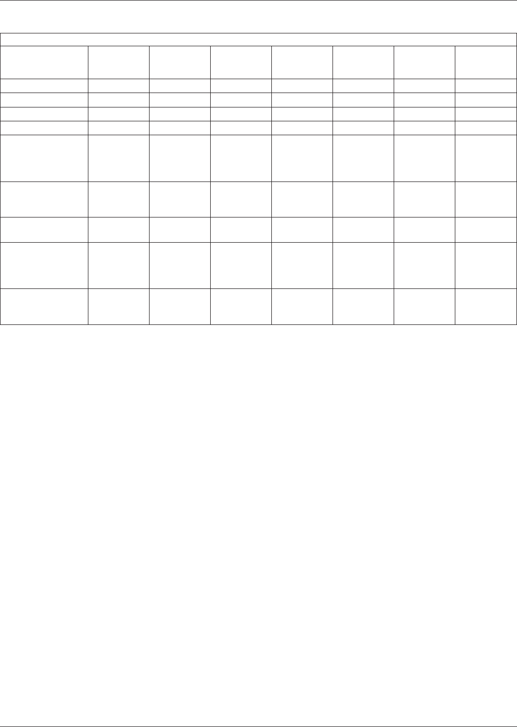
highly dependent upon the product application. In Table
3-1, typical worst case use environments for 9 product cat-
egories are given. These use environments should be
regarded as guidelines only; the actual use environment as
well as the environmental conditions of the SM assembly
being designed may be significantly different.
Table 3−1 Realistic Representative
(1)
Use Environments, Service Lives, and Acceptable Failure Probabilities for Surface
Mounted Electronics Attachments by Use Categories
Worst-Case Environment
Use Category
Tmin
°C
Tmax
°C
∆T
(2)
°C
Dwell Time
t
D
hrs Cycles/Year
Typical Years
of Service
Accept.
Failure
Risk
(3)
,%
Consumer 0 +60 35 12 365 1-3 ~1
Computers +15 +60 20 2 1460 ~5 ~0.1
Telecom -40 +85 35 12 365 7-20 ~0.01
Commercial Aircraft -55 +95 20 12 365 ~20 ~0.001
Industrial
and Automotive
Passenger
Compartment
−55 +96 20
&40
&60
&80
12
12
12
12
185
100
60
20
~10 ~0.1
Military
Grounds and
Ship
−55 +95 40
&60
12
12
100
265
~10 ~0.1
Space leo
geo
−55 +95 3 to 100 1
12
8760
365
5-30 ~0.001
Military a
Avionics b
c
Maintenance
−55 +95 40
60
80
&20
2
2
2
1
365
365
365
365
~10 ~0.01
Automotive
under hood
−55 +125 60
&100
&140
1
1
2
1000
300
40
~5 ~0.1
& = in addition
1 Does not cover all possible use environments, but only most common.
2 ∆T represents the maximum temperature swing, but does not include power dissipation effects for components; for reliability estimations the actual local tem-
perature swings for components and substrate, including power dissipation should be used.
3 The ‘Acceptable Failure Risk’ is the percentage of product in the field that has failed, due to wearout mechanisms, at the end of the ‘Typical Years of Service.’
IPC-D-279 July 1996
6

3.1.7 Environmental Stresses The operating life of a
surface mounted assembly is dependent upon a number of
factors which include intended usage, usage environments,
strength of the materials and components to withstand the
stresses imposed by the usage and the environments, mate-
rial (variables), etc. In a surface mounted assembly, the
most critical element from the life cycle viewpoint are the
solder joints and PTVs. Cyclic (or fatigue) displacements
experienced during various phases of the product’s life
cycle are responsible for consumption of useful life of
material elements.
One of the major contributors to the cyclic loading is ther-
mal cycling due to the internal power cycling and external
environmental changes. Another important contributor is
vibration during the operational use, transportation, han-
dling, etc. An estimate of the fatigue life of the solder
assembly that will be consumed by these fatigue cycles
during the product’s life cycle can be obtained by perform-
ing a cumulative damage analysis.
It should be noted that the cumulative damage analysis
requires the knowledge of fatigue characteristics of the
materials involved. Also, a thorough understanding of how
the product will be used, handled and maintained, by the
user and under what environments, is necessary. See
Appendix E.
3.1.8 Temperature/Thermal Temperature is one of the
most important parameters in the use environment that
must be considered in the SM PWA design process. Tem-
perature history is the most significant parameter affecting
the reliability of SM solder joints. For some product appli-
cations, the use environment consumes the most significant
portions of the required fatigue life; this is typically the
case where the product development cycle includes produc-
ing a prototype prior to the ‘‘final build.’’
Therefore, DfR depends to a large extent on the thermal
design for the assembly, as well as the external thermal
environment. Temperature is also important, since many
materials in electronic assemblies have properties which
change significantly with temperature.
3.1.9 Cyclic Temperature Swings Cyclic thermal excur-
sions, ∆T, cause thermal expansion mismatches due to dif-
ferent parts of the assemblies having materials with differ-
ent CTEs and/or being at different temperatures. Thus, the
size of the cyclic temperature swing is proportional to the
resulting loading. The larger the ∆T, the larger the threat to
reliability.
During cyclic temperature excursions, these cycles can
have different profiles, e.g., sinusoidal, trapezoidal, saw-
tooth, square-wave, etc. These differences are important in
understanding time-dependent and rate-dependent pro-
cesses. The transient parts of the profile give the ramping
rates of the temperature change which can cause transient
temperature gradients and over-stress conditions. The
steady-state, or near steady-state, parts of the profile deter-
mine the duration of the temperature dwells which are
important for time-dependent processes like creep and
stress relaxation.
3.1.10 Thermal Shock In thermal shock, the extremely
rapid temperature changes (∼30°C/minute and above)
result in warping of the surface mount assembly. The
warpage is caused by large transient thermal gradients
induced by the rapid temperature change when the boards
are plunged into a new thermal environment. The warpages
result in tensile and shear stresses where the tensile load-
ing dominates over the steady state expansion mismatch.
Thus, even assemblies with matched coefficients of thermal
expansion will exhibit solder joint failures when subjected
to thermal shock. The thermal shock loading mechanism is
summarized in Figure 3-1.
Thermal shock conditions can arise from several sources.
Examples of these are:
1) Rapid changes in external environment, e.g., sun-to-
shade in space, missile launch, wing-mounted avion-
ics, automobile start-up from very cold.
2) Rapid changes in power dissipation.
3) Various manufacturing/repair processes, e.g., reflow,
vapor degrease, rework, etc.
The distinction between thermal shock and thermal cycling
is not always addressed in designing reliability experi-
ments. There is a fundamental difference between thermal
shock and thermal cycling. The primary differences arise
from the mechanism of loading. Thermal shock tends to
result in multiaxial states of stress dominated by tensile
overstresses and tensile fatigue. On the other hand, as pre-
viously discussed, thermal cycling results in shear loads
and failure occurs from an interaction of shear fatigue and
stress relaxation.
Thermal shock is usually performed in dual chamber
arrangements or with liquid nitrogen injection whereas
thermal cycling is performed in single chamber cycling
equipment. Dual chamber arrangements will produce tem-
perature transition rates in excess of 50°C/minute.
Single chambers generally do not produce transition rates
even close to 30°C/minute which is the rate necessary to
induce thermal shock. The results of these two types of
testing are generally incompatible. Finally, thermal shock
testing for purposes of evaluating surface mount solder
joint reliability is only appropriate if thermal shock is
indeed a field condition encountered by the product.
In some specifications, the definitions of thermal cycling
and thermal shock are not fully differentiated; the rates of
change are more closely associated with what we are call-
ing thermal shock.
July 1996 IPC-D-279
7