IPC-D-279 EN.pdf - 第24页
inside the land area. If a ‘ ‘pads-only’ ’ approach is not fea- sible, then it is crucial that solder mask be applied for sur- face mount designs to act as a dam to solder migration. The ‘ ‘pads-only’ ’ approach has seve…
subsequent conductor temperature rise.
Minimum trace spacings should be reviewed keeping in
mind the influences of DC voltage and possible electro-
chemical migration, AC voltage and possible corona leak-
age currents, high humidity and possible electrochemical
migration, low air pressure and possible corona leakage
currents/premature voltage breakdown, and conductive or
corrosive contamination from the ambient. See IPC-D-275,
IPC-SM-782, and IPC-TR-476 and IEC 664.
3.3.7 PTH and PTV Thermal Isolation/Relief Large con-
ductor areas such as ground planes, power planes and ther-
mal planes ‘‘heatsink’’ PTH and PTVs to which they con-
nect. During the soldering or reflow process, the reduction
in local temperature can result in ‘‘cold’’ solder joints,
bridging or icicling and may require increased time at tem-
perature to affect a proper and reliable solder joint. Ther-
mal relief inner lands such as those depicted in Figure 3-2
provide a measure of thermal resistance between the exter-
nal soldered lands and the heatsinking plane. The results
are lower required reflow temperatures, less printed board
stress, and more consistent solder joints.
3.3.8 Test Pads Test pads are required for bare-board
test; see also IPC-ET-652. Previous techniques used to
implement digital PWA testability such as massive addition
of test nodes, become less feasible with the smaller dimen-
sions of SMT PWAs and the number of test nodes required
for components with 100-400 terminations; the mechanical
force exerted by test pins is sufficient to flex and break
components and solder joints.
Testability is a particular issue for field repair activities
where the full capabilities of the SM PWA may not be
exercised due to test equipment limitations or lack of avail-
able test time; Built-in-Test-Equipment, Built-in-Test,
Built-in-Self-Test (BITE, BIT or BIST) capabilities could
be invaluable in these circumstances or may be the only
alternatives. See section 8 and Appendix J.
Solder mask overlap or residue on test pads (whether by
design or by loss of process control) reduces test reliabil-
ity. (See IPC-D-275, and IPC-SM-782)
Provide adequate margin between the land and solder
mask.
Conformal coating on test pads results in diminished test
accessibility; testability buss methodologies and structures
may be required to permit effective and efficient fault cov-
erage. (See IPC-SM-782)
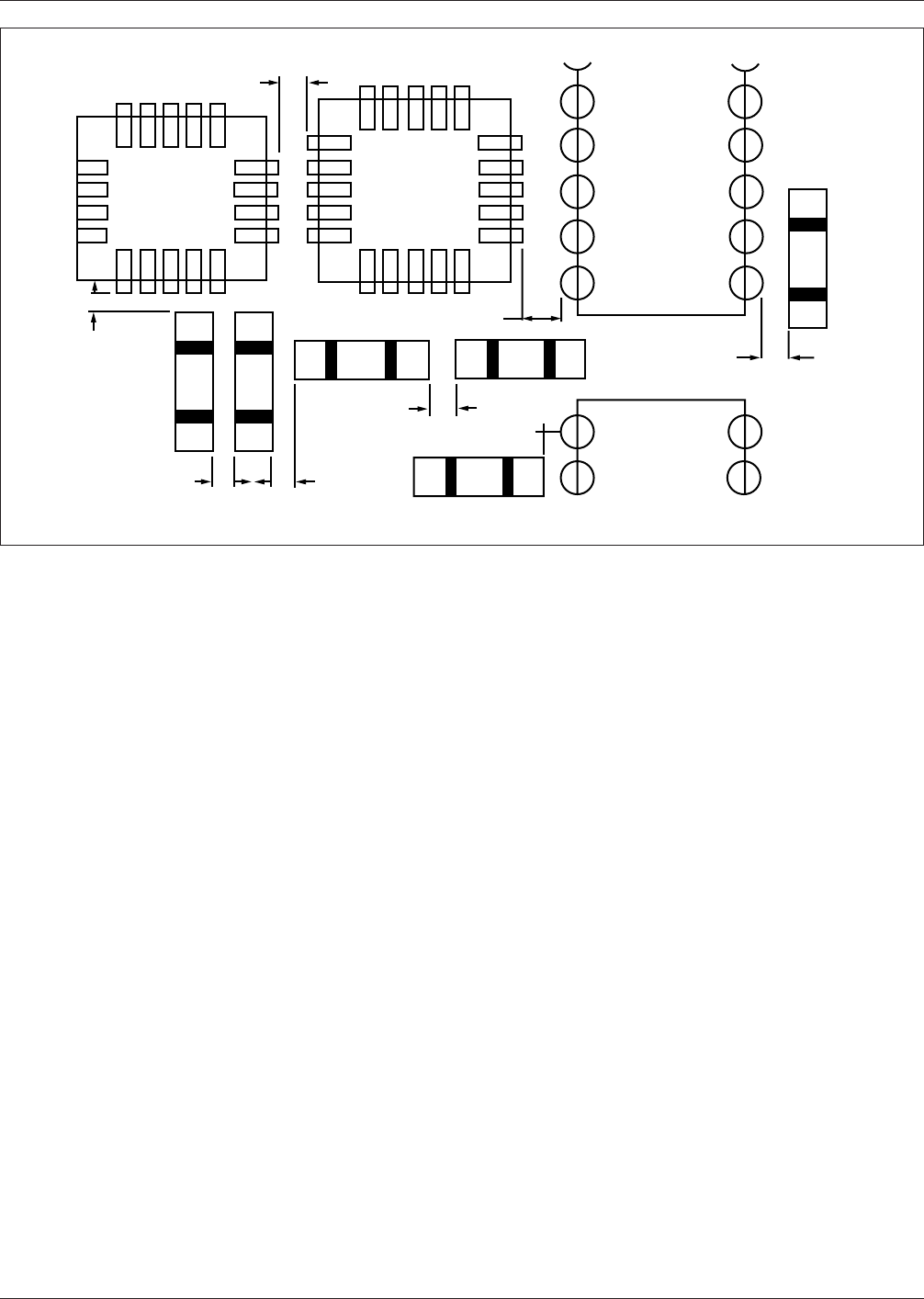
3.3.9 Spacing Between Parts The designer should pro-
vide for manufacturability, inspectability, testability and
repairability of SMT assemblies. A minimum interpackage
spacing is required to satisfy all these manufacturing
requirements. Some designs require that surface mount
components be positioned as tightly as possible (brick-
walled); these designs do not allow solder joint inspection.
See figure 3-3 and section 8.0.
3.3.10 ‘‘Pads-Only’’ Design For this reason, many mul-
tilayer military and space applications utilize a ‘‘pads-
only’’ outer layer design. By submerging all conductors
and power planes in the inner-layers, only the land areas
are exposed on the board surface. Connection to the sub-
layers is then accomplished by small plated and filled vias
IPC-279-04
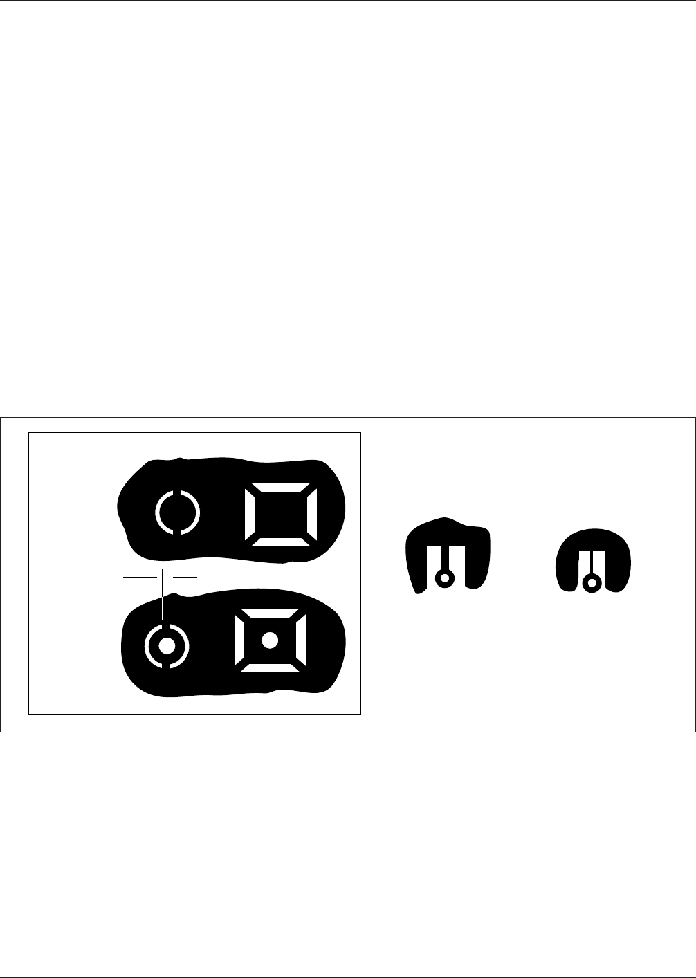
Figure 3−2 Thermal Relief in Ground Planes
Land Before
Drilling
Land
After Drilling
Wide Straps Narrow Straps
Web Width
▼
▼
IPC-D-279 July 1996
12
inside the land area. If a ‘‘pads-only’’ approach is not fea-
sible, then it is crucial that solder mask be applied for sur-
face mount designs to act as a dam to solder migration.
The ‘‘pads-only’’ approach has several advantages worth
noting:
• the construction is compatible with soldering pro-
cesses, conformal coatings and common cleaning sol-
vents.
• The electrical and dielectric performance is no differ-
ent than the remainder of the P/I structure. Stenciling
of solder paste is improved.
• Application of solder mask to flexible and flex-rigid
P/I structures may be difficult.
• Resolution of this approach is the same as the resolu-
tion of copper etching.
3.3.11 Components with Reduced Clearances (Traces
Under)
Excessively thick solder mask, particularly dry
film over traces under components with small clearance,
can contribute to the formation of crevices which entrap
flux. In the case where the solder mask touches the bottom
of the component, if insufficient solder paste is used, it may
result in chip component draw-bridging (tombstoning),
insufficient solder fillet or lack of solder joint. (See IPC-
SM-782 and IPC-D-275.)
3.3.12 Components with Reduced Clearance and Open
Vias
Components with reduced clearance should not be
over open vias, particularly if wave soldering is used. The
vias allow flux up under the component to be entrapped in
the reduced clearance space.
Heat dissipaters should generally be ‘‘upstream’’ of tall
components to avoid recirculation cells.
Where lower junction temperature T
j
is required, consider
the following avenues particularly applicable to SMT: ther-
mal vias, thermally conductive adhesives from component
to printed board, and power and ground planes included in
the thermal design. In addition, consider the following
moves: sensitive components ‘‘upstream’’ of power dissi-
paters, power dissipaters further apart to reduce power den-
sity, power dissipaters closer to cold wall (edge of card if
card clamps are used), and power dissipaters ‘‘upstream’’
of tall components.
Long, tall components such as connectors are ideally
placed parallel to the airflow. Placement of these compo-
nents perpendicular to the airflow results in the generation
of recirculation cells which reduce the heat transfer from
heat dissipaters or which increase heat transfer to heat sen-
sitive components.
3.4 Coefficient of Thermal Expansion (CTE) and CTE-
Mismatch
Electronic assemblies consist of a multitude of
elements of different materials. These materials have differ-
ent coefficients of thermal expansion (CTE), of which some
are listed in Appendix G. Some CTEs also vary with tem-
perature. Because of external temperature variations and
internal heat generation and different thermal resistances,
IPC-279-05
Figure 3−3 Spacing Between Parts
1.25 mm
0.63 mm
1.5 mm
0.63 mm
1.0 mm 1.0 mm
1.25 mm
1.5 mm
July 1996 IPC-D-279
13

different locations within an electronic assembly are typi-
cally at different temperatures.
Matching the CTEs at a joint is no guarantee of freedom
from the problem because electronic components are their
own heat sources and because there is a temperature differ-
ence between component and substrate. The problem is
directly related to the size of the component, the thickness
of the solder joint and the compliance of the lead. The
major problem arises from thermally induced cyclic stress
in the solder joint of the leadless ceramic chip carrier
(LLCCC) components. Some components are very easy to
assemble, test and repair; others are not. The availability of
a component, its performance data, its degree of testability,
its reliability and its compatibility with manufacturing and
assembly processes and equipment influences component
selection.
3.5 Solder Joint Reliability The reliability of the surface
mount solder attachment of components to the printed cir-
cuit boards depends on a number of different parameters.
Some of these parameters are under the direct control of
the designer, some can be influenced by the designer, and
some are beyond the control of the designer.
Also, some of these parameters have a very strong influ-
ence on reliability. Relatively small changes or inaccura-
cies in these primary parameters have a large impact on the
reliability. The impact of these parameters can be seen
from the reliability prediction Equations A-3 and A-4 in
Appendix A, Solder Joint Reliability.
3.5.1 Primary Design Parameters The following are
design parameters that have been identified as having a
primary (order of magnitude) influence on SM solder
attachment fatigue reliability.
3.5.1.1 Component Size The physical size of the com-
ponent determines the amount of displacement a solder
joint experiences during thermal expansion/contraction of
the component and the substrate to which it is soldered.
Larger components are larger threats to reliability. The
component size is determined by the number of I/Os and
the pitch.
3.5.1.2 Attachment Type The choice of attachment type
(leadless or leaded) determines the maximum stress level
that can be experienced in a solder joint during thermal
cycling. The stiff leadless attachments typically stress the
solder beyond the yield strength, whereas compliant leaded
attachments typically do not. This choice determines the
reliability model that needs to be applied and affects the
statistical failure distribution (Weibull slope). Leaded
attachments provide larger reliability margins, which
increase with decreasing lead stiffness. It needs to be noted
that lead compliance can vary greatly depending on the
lead geometry. Lead stiffnesses as high as 1100 N/mm for
SM connector header leads and as low as 1.5 N/mm for
fine-pitch S-leads have been determined.
3.5.1.3 Solder Joint Height The solder joint height
determines the strain level experienced in the solder joint
for a given component/substrate displacement. It results
from the solder-filled gap between the component metalli-
zation or component lead and the substrate pad. Higher
solder columns reduce the strains in the solder joints and
increase reliability. Solder joint height is not the height of
the fillet. For leaded attachments the solder joint height is
not a measurable quantity; it has been defined in terms of
the solder paste stencil thickness.
3.5.1.4 Solder Joint Area Solder joint area determines
the stresses in a solder joint resulting from a given compo-
nent/substrate displacement. It is of importance primarily
for compliant leaded attachments. Larger solder joint areas
reduce the applied stresses and increase reliability; how-
ever, the possible range of effective increase in area is very
limited.
3.5.1.5 Lead Stiffness The lead stiffness determines the
forces resulting from a given component/substrate dis-
placement. Because the corner solder joints experience the
largest displacements and the displacements are in the
direction of the component center (neutral point), it is the
diagonal lead stiffness which is of primary importance.
Lower lead stiffness results in increased reliability.
3.5.1.6 Coefficient of Thermal Expansion The linear
coefficient of thermal expansion (CTE or α) represents the
change in linear dimension of a material due to a change in
its temperature. Components and substrates consist typi-
cally of a variety of materials all having different CTEs; the
effective CTEs are a combination of the individual material
CTEs and typically are different in different directions of
components and substrates. CTEs need to be measured to
avoid possible large errors in the reliability predictions. See
Appendix G for CTE values of different materials.
3.5.1.7 CTE - Mismatch The CTE-mismatch (∆CTE or
∆α) is the difference between the coefficients of thermal
expansion (CTE) of two materials or parts joined together;
in most instances it is the CTE-mismatch between compo-
nent and substrate, the global expansion mismatch, that is
most important, while the CTE-mismatch between the sol-
der and the materials to which it is bonded (ceramic, alloy
42, Kovar ), the local expansion mismatch, plays a smaller,
but not negligible role. In some designs (ceramic compo-
nent on ceramic or silicone substrate), this local CTE-
mismatch assumes primary importance. Large CTE mis-
matches pose large reliability threats; the effect of power
dissipation within the component makes CTE matching not
IPC-D-279 July 1996
14