IPC-D-279 EN.pdf - 第47页
can be rather more complex [Ref. A-9: 9]. A-2.2 Global Expansion Mismatch The global expansion mismatches result from dif ferential thermal expansions of an electronic component or connec- tor and the printed board to wh…
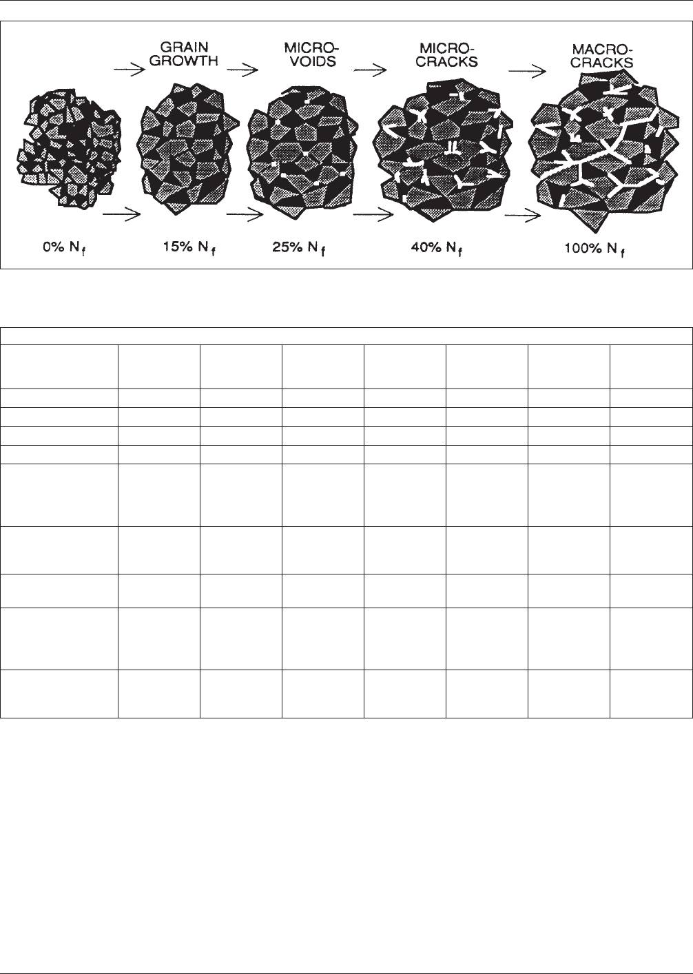
and all leaded solder joints, show localized damage con-
centrations with the damage shown in Figure A-1 preced-
ing an advancing macro-crack.
The solder joints frequently connect materials of highly
disparate properties, causing global thermal expansion mis-
matches [Refs. A-9: 1-6], and are made of a material, sol-
der, that itself has often properties significantly different
than the bonding structure materials, causing local thermal
expansion mismatches [Refs. A-9: 4,7].
The severity of these thermal expansion mismatches, and
thus the severity of the reliability threat, depends on the
design parameters of the assembly and the operational use
environment. In Table A-1 guidelines as to the possible use
environments for nine of the more common electronic
applications are illustrated [Refs. A-9: 8,9]. However, it
needs to be emphasized, that the information in Table A-1
should serve only as a general guideline; for some use cat-
egories the description of the expected use environment
Figure A−1 Depiction of the Effects of the Accumulating Fatigue Damage in Solder Joint Structure
Table A−1 Realistic Representative
(1)
Use Environments, Service Lives, and Acceptable Failure Probabilities for Surface
Mounted Electronics Attachments by Use Categories [Ref. A-9: 10]
Worst-Case Environment
Use Category
Tmin
°C
Tmax
°C
∆T
(2)
°C
Dwell Time
t
D
hrs Cycles/Year
Typical Years
of Service
Accept.
Failure
Risk
(3)
,%
Consumer 0 +60 35 12 365 1-3 ~1
Computers +15 +60 20 2 1460 ~5 ~0.1
Telecom -40 +85 35 12 365 7-20 ~0.01
Commercial Aircraft -55 +95 20 12 365 ~20 ~0.001
Industrial
and Automotive
Passenger
Compartment
−55 +96 20
&40
&60
&80
12
12
12
12
185
100
60
20
~10 ~0.1
Military
Grounds and
Ship
−55 +95 40
&60
12
12
100
265
~10 ~0.1
Space leo
geo
−55 +95 3 to 100 1
12
8760
365
5-30 ~0.001
Military a
Avionics b
c
Maintenance
−55 +95 40
60
80
&20
2
2
2
1
365
365
365
365
~10 ~0.01
Automotive
under hood
−55 +125 60
&100
&140
1
1
2
1000
300
40
~5 ~0.1
& = in addition
1 Does not cover all possible use environments, but only most common.
2 ∆T represents the maximum temperature swing, but does not include power dissipation effects for components; for reliability estimations the actual local tem-
perature swings for components and substrate, including power dissipation should be used.
3 The ‘Acceptable Failure Risk’ is the percentage of product in the field that has failed, due to wearout mechanisms, at the end of the ‘Typical Years of Service.’
July 1996 IPC-D-279
35

can be rather more complex [Ref. A-9: 9].
A-2.2 Global Expansion Mismatch
The global expansion mismatches result from differential
thermal expansions of an electronic component or connec-
tor and the printed board to which it is attached via the
surface mount solder joints. These thermal expansion dif-
ferences result from differences in the CTEs and thermal
gradients as the result of thermal energy being dissipated
within active components.
Global CTE-mismatches typically range from ∆α~2
ppm/°C (1 ppm=lx10
-6
) for CTE-tailored high reliability
assemblies to ~14 ppm/°C for ceramic components on
FR-4 printed boards. CTE-mismatches of ∆α <2 ppm/°C
are not achievable in reality as a consequence of the vari-
ability of the CTE values of the materials involved on both
components and printed boards.
Global thermal expansion mismatches typically are the
largest, since all three parameters determining the thermal
expansion mismatch—the CTE-mismatch, ∆α, the tem-
perature swing, ∆T, and the acting distance, L
D
—are large.
This global expansion mismatch will cyclically stress, and
thus fatigue, the solder joints. The cyclically cumulative
fatigue damage will ultimately cause the failure of one of
the solder joints, typically a corner joint, of the component
causing functional electrical failure that is initially intermit-
tent.
A-2.3 Local Expansion Mismatch
The local expansion mismatch results from differential
thermal expansions of the solder and the base material of
the electronic component or printed board to which it is
soldered. These thermal expansion differences result from
differences in the CTE of the solder and those of the base
materials together with thermal excursions [Refs. A-9: 4,7].
Local CTE-mismatches typically range from ∆α~7 ppm/°C
with copper to ~18 ppm/°C with ceramic and ~20 ppm/°C
with Alloy 42 and Kovar
TM
. Local thermal expansion mis-
matches typically are smaller than the global expansion
mismatches, since the acting distance, the maximum wetted
area dimension, is much smaller—in the order of hundreds
of ~µm.
A-2.4 Internal Expansion Mismatch
An internal CTE-mismatch of ~6 ppm/°C results from the
different CTEs of the Sn-rich and Pb-rich phases of the
solder. Internal thermal expansion mismatches typically are
the smallest, since the acting distance, the size of the grain
structure, is much smaller than either the wetted length or
the component dimension—in the order of less than 25 µm
[Ref. A-9: 11].
A-2.5 Solder Attachment Failure
The failure of the solder attachment of a component to the
substrate to which it is surface mounted is commonly
defined as the first complete fracture of any of the solder
joints of which the component solder attachment consists.
Given that the loading of the solder joints is typically in
shear, rather than in tension, the mechanical failure of a
solder joint is not necessarily the same as the electrical
failure. Electrically, the mechanical failure of a solder joint
results, at least initially, in the occasional occurrence of a
short-duration (<1 µs) high-impedance event during either
a mechanical or thermal disturbance. From a practical point
of view, the solder joint failure is defined as the first obser-
vation of such an event.
For some applications this failure definition might be inad-
equate. For high-speed signals with sharp rise times signal
deterioration prior to the complete mechanical failure of a
solder joint might require a more stringent failure defini-
tion. Similarly, for applications which subject the electronic
assemblies to significant mechanical vibration and/or shock
loading, a failure definition that considers the mechanical
weakening of the solder joints as the result of the accumu-
lating fatigue damage might be necessary.
A-3.0 RELIABILITY PREDICTION MODELING
A-3.1 Creep-Fatigue Modeling
It has been experimentally shown [Refs. A-9: 2,4,12,13]
that the fatigue life of surface mount solder joints can be
described by a power law similar to the Coffin-Manson
low-cycle fatigue equation [Ref. A-9: 14] developed for
more typical engineering metals. For practical reasons and
as the direct consequence of the time-dependent stress-
relaxation/creep behavior of the solder at typical use envi-
ronments (see Table A-1), the specialized case of the
Coffin-Manson equation requires reversion to the more
general strain-energy relationship of Morrow [Ref. A-9:
15]; it also requires that the cyclic strain energy be based
on the total possible thermal expansion mismatch and that
the exponent is a function of temperature and time to pro-
vide a measure of the completeness of the stress-relaxation
process. The Engelmaier-Wild solder creep-fatigue equa-
tion [Refs. A-9: 1-6,9,12], subject to some caveats listed
later, relates the cyclic visco-plastic strain energy, repre-
sented by the cyclic fatigue damage term, ∆D, to the
median cyclic fatigue life for both isothermal-mechanical
and thermal cycling [Ref. A-9: 16]
N
f
(50%)=
1
2
[
2e’
f
∆D
]
−1
c
[Eq. A-1]
where
e’
f
= fatigue ductility coefficient, =0.325 for eutectic and
60/40 Sn/Pb solder (for other solders the value of e’
f
is expected to be somewhat different).
IPC-D-279 July 1996
36

Solder, uniquely among the commonly used engineering
metals, readily creeps and stress-relaxes at normal use tem-
peratures; the rate of creep and stress-relaxation is highly
temperature- and stress-level-dependent. Thus, the cyclic
fatigue damage term, ∆D, for practical reasons, has to be
based on the total potential damage at complete creep/
stress relaxation of the solder. For cyclic conditions that do
not allow sufficient time for complete stress relaxation ∆D
is larger than the actual fatigue damage. The temperature-
and time-dependent exponent, c, compensates for the
incomplete stress relaxation and is given by
c =−0.442 − 6x10
−4
T
SJ
+ 1.74x10
−2
ln(1 +
360
t
D
)
[Eq. A-2]
where
T
SJ
= mean cyclic solder joint temperature
t
D
= half-cycle dwell time in minutes.
The half-cycle dwell time relates to the cyclic frequency
and the shape of the cycles and represents the time avail-
able for the stress-relaxation/creep to take place.
In Eq. A-1 the exponent is given as (−1/c), which is men-
tally confusing; this format exists for historical reasons in
that the underlying work [Refs. A-9: 14,15] was always
stated this way. For typical electronic applications (T
SJ
=0
to 100°C and t
D
= 15 to 720 minutes) the exponent (−1/c
ranges between 2.0 and 2.6.
Equations A-1 and A-2 come from a generic understanding
of the response of SM solder joints to cyclically accumu-
lating fatigue damage resulting from shear displacements
due to the global thermal expansion mismatches between
component and substrate. These shear displacements cause
time-independent yielding strains and time-, temperature-,
and stress-dependent creep/stress relaxation strains. These
strains, on a cyclic basis, form a visco-plastic strain energy
hysteresis loop which characterizes the solder joint
response to thermal cycling and whose area, given as the
damage term ∆D, is indicative of the cyclically accumulat-
ing fatigue damage. Hysteresis loops in the shear stress-
strain plane have been experimentally obtained [Refs. A-9:
13,17-19].
A-3.2 Damage Modeling
The assessment of the cyclically cumulating fatigue dam-
age is not a straight-forward task. While Eq. A-1 is widely
used, the question of how to best quantify the cyclic fatigue
damage is still hotly debated. The choices are primarily
between more complex finite-element analyses (FEA),
which can give more detailed information and can include
second-order effects, but require a large number of not
fully-supported assumptions [Ref. A-9: 20]; and closed-
form empirically-based relationships of the first-order
design parameters, which cannot include second-order
effects and have use limitations due to their simple nature,
but allow, due to their simple form, a direct assessment of
the impact of the primary design parameters as well as
design trade-offs.
The following cyclic fatigue damage terms are of the sim-
plified closed-form type and should be utilized with the
application caveats that follow [Refs. A-9: 1-6,9,12,16,21].
The cyclic fatigue damage term for leadless SM solder
attachments, for which the stresses in the solder joints
exceed the solder yield strength and cause plastic yielding
of the solder, is
∆D(leadless)=
[
FL
D
∆(α∆T)
h
]
[Eq. A-3]
For solder attachments with leads compliant enough, so
that the solder joint stresses are below the yield strength
and thus are not bounded by it, the cyclic fatigue damage
term is
∆D(leaded)=
[
FK
D
[L
D
∆(α ∆T)]
2
(919 kPa)Ah
]
[Eq. A-4]
where for English units the scaling coefficient is 133 psi
instead of 919 kPa.
Equation A-4 contains the design parameters that have a
first-order influence on the reliability of SM solder attach-
ments. They are
A = effective minimum load bearing solder joint
area;
F = empirical ‘‘non-ideal’’ factor indicative of
deviations of real solder joints from idealizing
assumptions and accounting for secondary and
frequently intractable effects such as cyclic
warpage, cyclic transients, non-ideal solder
joint geometry, different solder crack propaga-
tion distances, brittle IMCs, Pb-rich boundary
layers, and solder/bonded-material expansion
differences, as well as inaccuracies and uncer-
tainties in the parameters in Eqs. A-1 through
A-4; 1.5>F> l.0 for ball/column-like leadless
solder joints (C4, C5, BGAs, CGAs),
1.2>F>0.7 for leadless solder joints with fillets
(castellated chip carriers and chip compo-
nents), F≈1 for solder attachments utilizing
compliant leads;
h = solder joint height;
K
D
= ‘‘diagonal’’ flexural stiffness of unconstrained,
not soldered, corner-most component lead,
determined by strain methods [see Refs. A-9:
22-25] or FEA;
L
D
= maximum distance between component solder
joints measured from component solder joint
July 1996 IPC-D-279
37