IPC-D-279 EN.pdf - 第20页
2. Metallic isolators including springs, metal meshes or wire rope; the latter provide smooth friction damp- ing. There are also other isolators such as viscous dampers which are velocity-sensitive. For high-frequency vi…
3.1.11 Electrical
3.1.11.1 ESD Susceptibility and Damage Prevention
All electronic components containing thin conducting or
insulating films are susceptible to electrostatic discharge
(ESD) damage. These components include those fabricated
in high speed technologies (MOS, bipolar, GaAs), thin film
technologies (resistors, integrated circuits, magnetic heads,
MOS capacitors), and in future, wafer scale integration and
multichip modules.
3.1.12 EMC/EMI The electromagnetic spectrum is usu-
ally divided into categories ranging from the long-
wavelength radiation from power lines through radio, infra-
red, visible, ultraviolet, and x-rays, to gamma rays at the
short-wave end. All electromagnetic waves consist of an
electric field and a magnetic field. The relative magnitude
of these fields depend on the emitter (EM source), wave
propagation medium, and the proximity of the emitter to
the subject assembly.
Many electronic circuits are susceptible to electromagnetic
radiation and must be shielded to ensure proper operation.
One of the most important effects of the electromagnetic
radiation in the environment is electromagnetic interfer-
ence (EMI). EMI is the electro-magnetic disturbances that
impair the desired signal. In practice, EMI is often divided
into two categories: conducted EMI and radiated EMI.
Conducted EMI is an interfering signal resulting from an
undesirable voltage or current coupled into a signal or
other pertinent conductor. Radiated EMI is an interfering
signal resulting from an electric and/or magnetic field
amplitude and frequency spectra intentionally or uninten-
tionally radiated by an electrical source. Examples of radi-
ated emission sources are radio and TV transmitters, light-
ning, digital system noise from electronic control systems,
etc. In military applications, an important effect is the inter-
action of electromagnetic radiation with electroexplosive
devices used as detonators. Improper EMI could acciden-
tally initiate the explosion.
EMC is the ability of electronic systems to operate in the
intended electromagnetic environment at designed levels of
performance and efficiency. The most direct approach to
protection is, in most cases, to avoid the limited region in
which high radiation levels are found. When exposure can-
not be avoided, shielding is the important protective mea-
sure. The material selected for shielding can be an impor-
tant factor. Ideal materials include steel, copper and nickel
coating. In the design process, apertures for cooling venti-
lation and cable connections on the shielding box should be
properly designed so that the EMI will have no influence
inside the shielded space.
3.1.13 Mechanical Shock and Vibration Shock and
vibration are common accelerators of failure in electronic
packaging. The most frequent vibration-induced failures in
surface mount are:
1. Flexing of leads and interconnects.
2. Dislodging or damaging of parts and structures.
Methods have been developed to counter the destructive
effects of shock and vibration. Generally, isolation of a
printed board against the effects of shock and vibration
requires that the natural frequency of the printed board be
substantially lower than the undesired frequency of vibra-
tion to avoid the resonance.
The basic system level isolators available are:
1. Natural or synthetic rubber, used to damp the vibra-
tion.
IPC-279-03
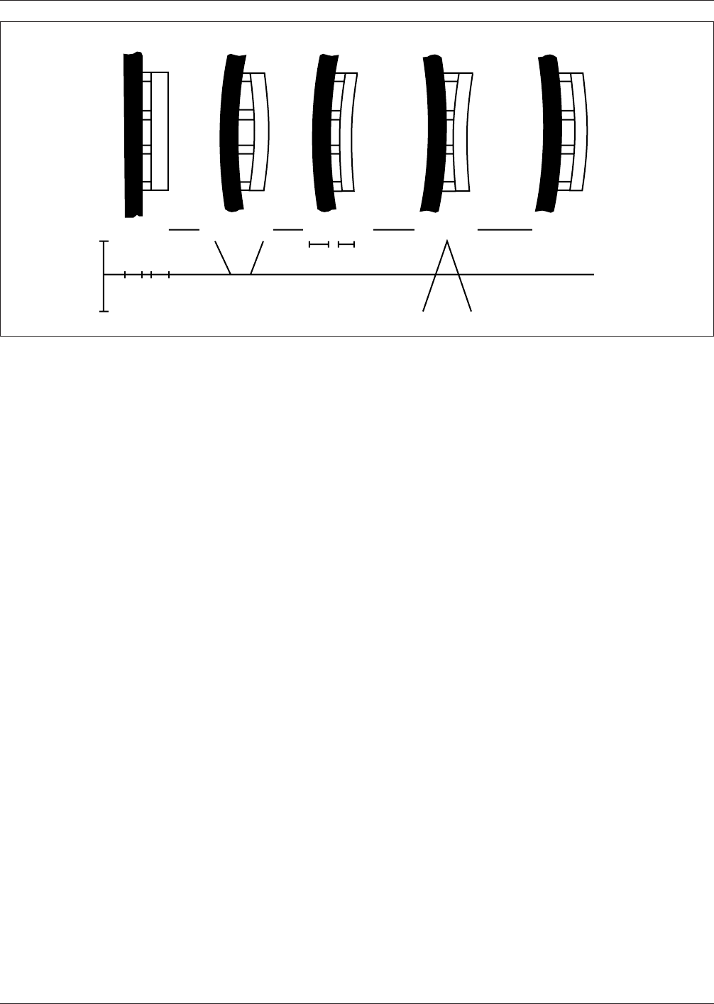
Figure 3−1 SMT Assembly Response to Thermal Shock
THERMAL
STEADY
STATE
THERMAL
STEADY
STATE
+ 125°CAT – 65°C
+ 125°C
AT
– 65°C
IPC-D-279 July 1996
8

2. Metallic isolators including springs, metal meshes or
wire rope; the latter provide smooth friction damp-
ing.
There are also other isolators such as viscous dampers
which are velocity-sensitive. For high-frequency vibration,
viscous dampers tend to become ineffective.
There are two approaches that may be taken when shock
and vibration are present: either isolate the printed board or
design it to withstand the shock and vibration. Studies have
shown that the ideal goal is to design equipment to be
resistant to shock and vibration, rather than to isolate it
from these forces.
Because the surface mount components are generally
smaller compared to the through-hole counterparts, they
are more vibration resistant due to the lower inertia. As the
PWA vibrates, the components mounted on the board are
subject to stress from two different effects. First, the mass
of the components is subjected to an acceleration that pro-
duces a force. The body of the component is kept in equi-
librium with reactive forces developed in the leads. Sec-
ond, the printed board flexes, which tends to bend the leads
back and forth at their joints with the board. Because of the
shorter lead lengths in SMT, the mechanical stress induced
by shock and vibration in leads is considerably smaller
compared to that in through-hole leads.
To detect/precipitate the flaws, stress screening with ran-
dom vibration should be performed. Usually, stress screen-
ing should be designed so that it causes minimal damage to
properly designed printed boards. This requires careful
determination of the screening intensity.
Depending upon the applications, the frequency ranges are
very different. For instance, the range for submarine elec-
tronic equipment is about 4-34 Hz, but for avionics the
range is 15-2000 Hz.
The following considerations must be included in the
analysis design for shock and vibration:
1. The location of the surface mount components rela-
tive to the supporting structure (i.e., edge, corner, or
center of the supporting structure).
2. The orientation of the components with respect to the
anticipated direction of the shock or vibration forces.
3. The maximum deflection of the printed board.
Mechanical shock to, and flexure of, a SM Printed Wiring
Assembly can occur during its life cycle. Each incident
could be characterized by the energy to be absorbed by the
assembly, the shock peak amplitude, duration and time rate
of change for correlation to sample shock testing:
• PWA struck by tooling during assembly (component
insertion or placement, riveting, testing, test fixtures,
probing, or depanelling)
• PWA installed into a card carrier or motherboard
• PWA dropped on a hard bench or floor
• Assembly dropped on a hard bench or floor
• Boxed product bounced and jolted during transporta-
tion
• Boxed product dropped on a hard bench, floor, truck
bed
• Product (in use) dropped on a hard work surface or
floor
• Product (in use) struck by passing equipment
• Product stored in racks, PWA fixtures, or rework sta-
tion grips.
• PWA subjected to combined environmental stress in
field use.
The assessment of the potential quality/reliability degrada-
tion of a printed wiring assembly (PWA) resulting from
exposure to the use environment cannot always be deter-
mined by considering each environmental stress in isola-
tion. For instance, consider the non-linear combined effects
of severe thermal and vibration stress application. A given
magnitude of random vibration at elevated temperature
(near or above T
g
) may produce increased PWA flexure
because of increased board softness or flexibility. Simulta-
neously, solder joint pull strength is decreased at the
elevated temperature. The result may be overload, that is, a
PWA configuration for either the elevated temperature or
the vibration applied at room ambient temperatures may
fail prematurely in service when exposed to the two factors
together. Board stiffness and damping as discussed in sec-
tion 4.0 are key factors to be considered. The adequacy of
a proposed design may require combined-environment
stress testing of prototypes prior to full-scale production.
See also the references by Steinberg and Engel regarding
vibration, shock and thermomechanical effects on PWA,
section 9.16.
3.1.14 Insulation Resistance
The emerging advanced technologies are characterized by
denser packaging resulting in ever finer conductor line
widths and spacings. Without changes in the material and
the operating environment, which for economic and practi-
cal reasons are not likely, finer lines and spacings result in
reduced insulation resistance and increased threat of CAF
(conductive anodic filament) formation. The DfR principles
listed in Appendix C need to be kept in mind in the design
and application of these emerging technologies.
The damage mechanisms work generally in two distinct
regions: at the surface and in the bulk of the electronic
assemblies, particularly the printed board. The measured
insulation resistance will depend upon the nature of the
laminate, solder mask and/or conformal coating under
investigation. It will also depend upon the degree of cure
of the polymers and for printed boards on the quality of the
drilling process for the plated-through holes (PTHs) and
vias (PTVs), and will be affected by soldering flux/paste
July 1996 IPC-D-279
9

residues if they dissolve into the polymeric material during
the soldering and/or cleaning processes.
3.1.15 Solvent Compatibility Surface Mount printed
wiring Assemblies (PWA) are subjected to solvents (includ-
ing water) and chemicals during manufacture, rework,
repair and service. These agents include those used in sol-
dering (alcohols, glycols and other solvents in flux vehicles
at temperatures approaching 150°C), in cleaning the assem-
bly after solder (saponifiers, neutralizers, hot water, ter-
pene, mixtures, hydrochlorofluorocarbon (HCFC) mixtures
and other halogenated solvents and blends at moderate pro-
cess temperatures), during removal of conformal coatings
with various chemicals, and during service (hydraulic and
cooling fluids and fuels in military applications; alcohols
and halogenated hydrocarbons during cleanup). These sol-
vents and chemicals can adversely affect the solder mask
(SM), printed wiring board, conformal coating, printed
board or component legends and markings as well as
degrade thin or mechanically stressed sections of plastic
components. See Appendix I.
3.1.16 Corrosion The result of corrosion is material loss
of the metallic conductors, permanent or intermittent con-
tinuity loss due to build up of non-conductive corrosion
residues (particularly between contacts) and permanent or
intermittent shorts due to build up of conductive corrosion
residues and conductive metal dendrites. Corrosion accel-
erates the failure of components under cyclic fatigue con-
ditions.
The oxides of tin, nickel and copper are not good conduc-
tors. Low interfacial pressure contacts to these metals can
become resistive or intermittent. See Appendix L for
details.
3.1.17 External Radiation External radiation typically
includes X-Rays, β-particles and cosmic rays. It affects the
semi-conductor material through the generation of hole-
electron pairs in the bulk of the device. The purpose of
understanding the radiation effects is to enable the develop-
ment of radiation-hardened devices.
External radiation affects the different semiconductor
devices in different ways. For instance in bipolar types,
radiation causes an increase in low-frequency noise, high
leakage current across the p-n junctions, and a reduction in
current gain; in MOS types, a threshold voltage shift, a
reduction in transconductance and an activation of parasitic
elements are observed. See Appendix E.
3.1.18 Space Environment The space environment pre-
sents an unusual set of conditions which requires careful
evaluation (low air pressure, low gravity, low temperature
and radiation). See Appendix O.
3.2 Thermal Design The primary thermal parameter
which the designer must address is the temperature of the
junction or active film of the component; both the absolute
maximum or peak temperature and the steady state operat-
ing temperature limits imposed by the component manu-
facturer (as modified by derating protocols) must be
observed. The secondary thermal parameter is the solder
joint temperature since long service times at high tempera-
tures will result in grain growth in the solder, growth of the
intermetallic compound layers; and large temperature
swings in service will subject the joint to conditions lead-
ing to cyclic fatigue. See Appendix D for details.
Variation of the external (outside of the equipment enclo-
sure) ambient temperature is one of the multitude of factors
that will determine the actual temperature cycle a specific
surface mounted device will see in operation. Very simple
equipment, powered continuously at constant power will
see the same temperature swings as the external ambient.
In some cases, the system designer introduces built-in
means of reducing the temperature swing inside the cabi-
net, such as fans activated when the inlet air temperature
exceeds certain limits or inlet air heaters which are
activated when inlet air temperature drops below certain
limits.
In many applications, the variation of the temperature
inside the electronic enclosure is generated by variations of
the power dissipated by the electronics itself. Examples of
this type of behavior are on/off periods for the systems, and
fluctuations in the power dissipation as in telecommunica-
tion equipment due to variations in the number of simulta-
neous calls passing through the system.
It follows that different devices inside the same system
might be subjected to very different temperature cycles. In
order to assess the reliability of the solder joints, the
designer must perform a complete thermal analysis at the
device level.
In most applications, the temperature variations at a par-
ticular component in a system result from a combination of
system-external and system-internal temperature variations
combined with power dissipation fluctuations within the
component.
3.3 Printed Board Design and Layout The printed board
design and layout task, particularly for surface mount tech-
nology (SMT), has become more difficult and complex.
The difficulty of SMT designs has increased with the
increase in conductor density as a result of decreases in
termination pitch, conductor width and conductor spacing.
The complexity of SMT designs has increased with the
need to consider:
a) thermo-mechanical effects such as solder joint reli-
ability (see section 3.4, 3.6 and Appendix A)
b) testability and inspectability (see section 8 and
IPC-D-279 July 1996
10