Utah-94-721002-System-Manual.pdf - 第156页
mä~ëã~ä~Ä = lñÑç êÇ=fåë íêìãÉåí ë=m ä~ë ã~=qÉÅÜåçäçÖó= System Manual (2) The helium setpoint should be set so that there is 1-2 mTorr chamber pressur e with a wafer in place. This ensures that there is sufficient cooling…

System Manual= lñÑçêÇ=fåëíêìãÉåíë=mä~ëã~=qÉÅÜåçäçÖó= mä~ëã~ä~Ä
(h) Troubleshooting:
Check the backs of wafers for excessive contamination, scratching or curvature/bowing. Vent
chamber and check electrode for particles, scratches, or erosion. Check wafer clamp integrity and
wafer clamping force i.e. can you move the wafer by finger pressure when clamped?
Compare results with blank Si if possible. If blank Si is OK, there is a problem with the customer
wafers, i.e. they are warped or too flexible or too thin (thin wafers may require reduced He
pressure to avoid flexing of wafers), or the clamp ring does not have sufficient clamping points to
maintain wafer flatness.
Also check that the measured He pressure is correct – if the Helium pressure gauge is faulty, the
actual pressure could be far too high. Typical CM gauge pressure when wafer is clamped and
helium pressure applied (APC fully open and no other gases flowing) is in the range 0.3-2mT for
the range of Helium pressures given above.
For the range of helium pressures given previously: Typical CM gauge pressure when the wafer is
clamped and the helium pressure applied (with the APC fully open and no other gases flowing) is
in the range 0.3mTorr to 2mTorr.
Checks with the system vented:
(1) Ensure that the electrode is very flat and clean (no bumps or grooves eroded into it) and that the
back of the wafer is clean and smooth (no resist or glue or anything else adhering to the back),
and is mechanically strong so that it does not buckle or bow.
(2) Check that the wafer lift star (or pins) retracts fully below the surface of the electrode. This can be
checked with a flat edge placed on top of the star - if it wobbles then the star is too high. If the
star sticks up above the electrode, the helium will escape and the cooling efficiency will be
severely reduced (also, because of the increased gap between wafer and electrode surface, which
needs to be a few tens of microns for best cooling).
(3) Check that the clamping ring is actually clamping the wafer to give maximum clamp force. Often,
there can be a discrepancy between the wafer clamp recess height and the wafer thickness,
meaning that the wafer is not clamped and 'rattles' about inside the clamp ring. The clamping
force should therefore be adjusted as described in Section 6. of the system manual.
You should try to move the wafer with your finger, if you can move it then it is not clamped
properly and you may need to temporarily modify the ring by adding strips of PTFE or aluminium
foil to make it press down on the wafer.
(4) The wafer should be placed centrally in the clamp ring.
(5) Press down on the wafer in various places and see if it moves. This will indicate that the wafer is
not sitting down flat on the electrode. Try polishing away any bumps.
Checks with the system under vacuum:
(1) A good test of whether the wafer is being clamped properly is to measure the helium pressure in
the chamber (measured on CM gauge) both with and without a wafer in place for a variety of
helium pressure setpoints.
There should be a clear difference between helium pressure with and without wafer. If there is no
difference then it indicates that there is a helium leak caused by incorrect clamping.
Process Information (Information contained in this document is confidential)
Printed: 08 January 2006 09:37 Page 13 of 30 Issue 1: December 03
mä~ëã~ä~Ä= lñÑçêÇ=fåëíêìãÉåíë=mä~ëã~=qÉÅÜåçäçÖó= System Manual
(2) The helium setpoint should be set so that there is 1-2 mTorr chamber pressure with a wafer in
place. This ensures that there is sufficient cooling. It is probably best to work at as high a level as
you can tolerate if there is any doubt over cooling efficiency.
PKOKV= d~ëÉë=ïáíÜ=äçï=î~éçìê=éêÉëëìêÉ=
Gases with a low vapour pressure (e.g. SiCl4, BCl3) present unique problems for the gas supply system, e.g.
temperature dependence of gas pressure, condensation in the gas lines, and low line pressure.
To avoid the loss of line pressure during cold weather, it is recommended that gases with a low vapour
pressure are sited indoors, inside an extracted gas cabinet. However, it is NOT recommended to
deliberately heat the gas cylinder (e.g. by using a heated jacket) as this will result in the re-condensation
of the gas in the gas line and/or MFC, since these areas are likely to be cooler than the cylinder. The
presence of condensed gas in the gas line or MFC will cause loss of flow or severe pulsing of measured gas
flow.
Note that condensation problems can sometimes be observed even without direct cylinder heating. This is
usually due to a slight temperature difference between cylinder and MFC. In such cases, it is
recommended that heating tape is placed around the MFC, filter and valve assembly of the gas line to
ensure that the MFC and other components are kept at a higher temperature than the gas cylinder. An
alternative solution would be to use a heated MFC.
PKOKNM= båÇéçáåí=ÇÉíÉÅíáçå=íÉÅÜåáèìÉë=
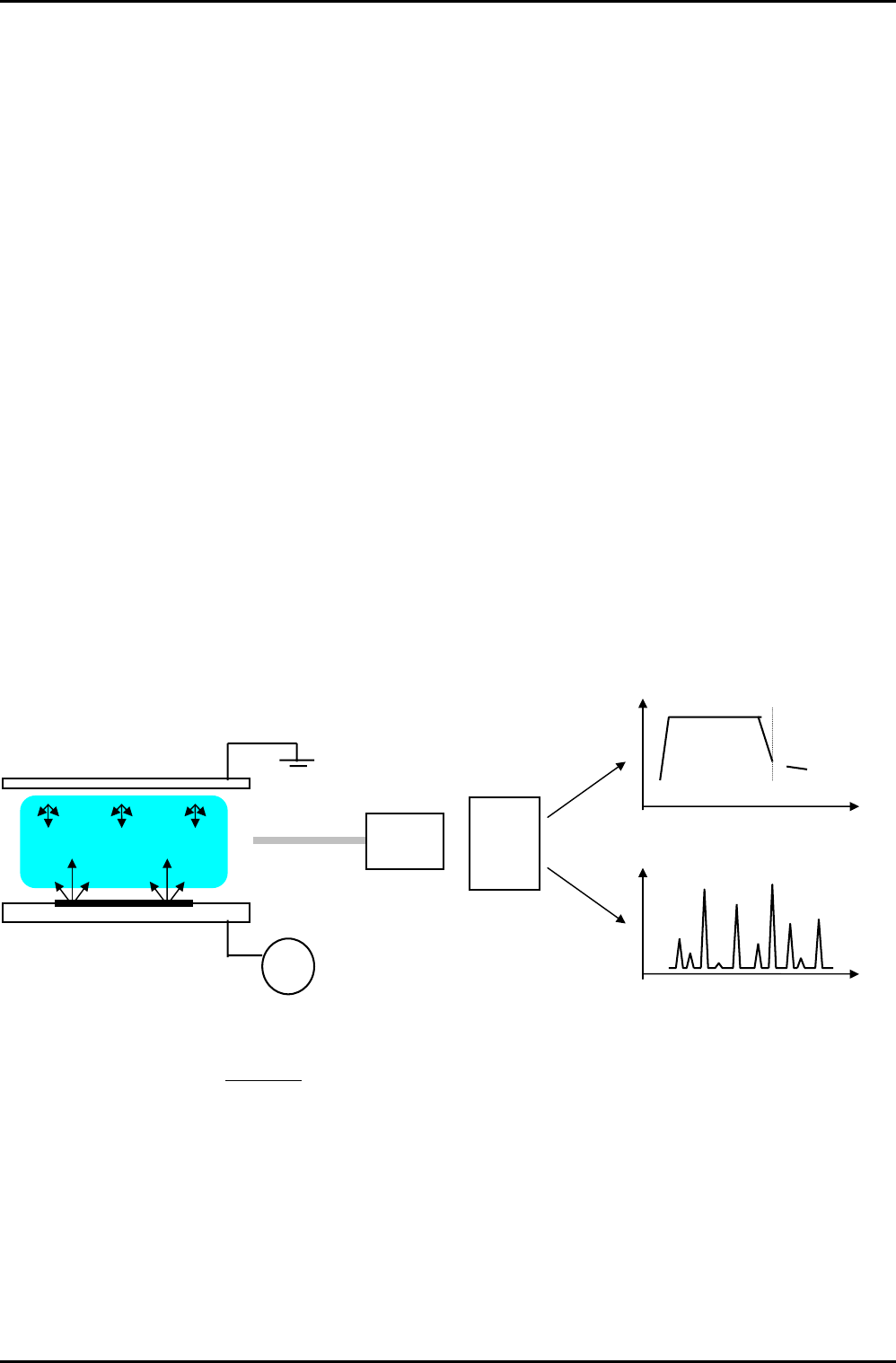
PKOKNMKN= léíáÅ~ä=Éãáëëáçå=ëéÉÅíêçëÅçéó=
Endpoint
Light
o/p
Monochromator
Light
o/p
RF
Reactive
s
p
ecies
Etch by-
products
PC
Etch time
Process chamber
Wavelength
• Monitoring of reactive species or etch by-products provides endpoint signal.
• Endpoint relies on etch stop layer.
• Scanned monochromator allows full spectrum analysis.
Process Information (Information contained in this document is confidential)
Issue 1: December 03 Page 14 of 30 Printed: 08 January 2006 09:37
System Manual= lñÑçêÇ=fåëíêìãÉåíë=mä~ëã~=qÉÅÜåçäçÖó= mä~ëã~ä~Ä
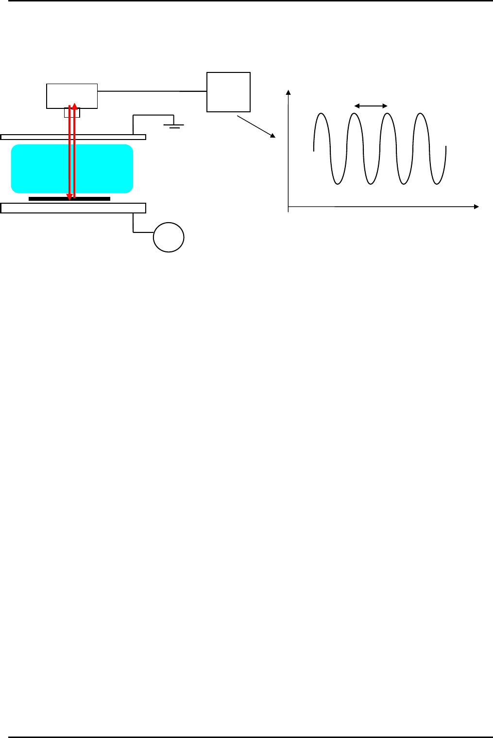
PKOKNMKO= i~ëÉê=áåíÉêÑÉêçãÉíêó=
RF
Process Chamber
Laser
Camera
Signal
Tim
e
PC
Process chamber
• In-situ etch rate monitoring
• Endpoint does not require etch stop layer
• Endpoint can be chosen anywhere within the layer once etch rate has been established.
PKOKNMKP= `çãé~êáëçå=çÑ=lbp=~åÇ=ä~ëÉê=ÉåÇéçáåí=íÉÅÜåáèìÉë=
A laser interferometer (LI) endpoint system has the benefits that it gives very precise measurement of etch
depth in the etched layer or layers and can be used on very small pieces of wafer.
It works best with a flat transparent layer (or stack of layers) on a reflective substrate.
It can be used to determine when the etch reaches an interface between differing materials (by detecting
a change in slope of the laser reflectance signal with time), or can measure the etch depth when partially
etching through a layer (by counting interference ripples).
It can also often be used to identify multiple interfaces when etching through different layers in a multi-
layer stack of materials (through the changes in reflectance of the materials in question).
The disadvantage is that the laser spot needs to be aligned every time to a suitable measurement point
on the wafer (i.e. an etched area, not a masked area). Also, it only measures a single point, so any process
non-uniformity will result in a range of etch depths across-wafer or across batch.
The optical emission spectroscopy (OES) system has the benefit that it does not require alignment for
every run, it simply looks at optical emission from the whole plasma. This however, means that it needs
larger wafers or a larger etched area (>2cm
2
) to effectively determine endpoint. The size of the etched
area needed for good OE endpoint is also dependent on the materials being etched since the emission
lines for certain materials can be very faint. Also, if the etch rate of the material is low then the
concentration of its etch species will be low.
OE can only detect a change in the strength of a particular emission line (or group of emission lines), so
can only detect when the etch passes through an interface between differing materials.
OE can give a qualitative idea of uniformity, since the length of the transition of the signal from before
endpoint to after endpoint will indicate the quality of the etch uniformity. Also the endpoint is more
accurate for the whole (average) of the wafer rather than a single point on the wafer.
Process Information (Information contained in this document is confidential)
Printed: 08 January 2006 09:37 Page 15 of 30 Issue 1: December 03