CP643E.pdf - 第84页
FK-9F98-05 CP- 643E Training Text for Service Engineers Edition 5.0 Chapter 5. Loader and Conveyor Adjustment [ 21 / 28 ] Fuji Machine Mfg. Co., Ltd. Okazaki SMT Equipment Quality Assurance Dept. Technical Support Div. S…

FK-9F98-05 CP-643E Training Text for Service Engineers
Edition 5.0 Chapter 5. Loader and Conveyor Adjustment [20/28]
Fuji Machine Mfg. Co., Ltd. Okazaki
SMT Equipment Quality Assurance Dept.
Technical Support Div. Section No.2
5-
20
<I/O → Standard → IN>
Sensor Location
LX005 IN-CONVEYOR MID-STOPPER UPPER LIMIT CHECK
LX006 IN-CONVEYOR MID-STOPPER LOWER LIMIT CHECK
LX003 (5) IN-CONVEYOR 1 SPEED DECELERATION POINT
LX004 (6) IN-CONVEYOR 1 PANEL ARRIVAL CHECK
LX008 (2) IN-CONVEYOR 2 SPEED DECELERATION POINT
LX009 (3) IN-CONVEYOR 2 PANEL ARRIVAL CHECK
LX007 (4) PANEL INTERVAL BETWEEN IN-CONVEYOR 1 AND 2
LX017 (1) IN-CONVEYOR PANEL IN
LX018 (8) IN-CARRIER FORWARD LIMIT PANEL CHECK (1)
LX019 (7) IN-CARRIER FORWARD LIMIT PANEL CHECK (2)
OUT-CONVEYOR MID-STOPPER UPPER LIMIT CHECK
OUT-CONVEYOR MID-STOPPER LOWER LIMIT CHECK
LX00E (13) OUT-CONVEYOR 1 PANEL ARRIVAL CHECK
LX00F (11) OUT-CONVEYOR 2 PANEL ARRIVAL CHECK
LX00C (12) PANEL INTERVAL BETWEEN OUT-CONVEYOR 1and 2
(14) OUT-CONVEYOR UNLOADER PANEL ARRIVAL CHECK
LX038 (10) OUT-CARRIER FORWARD LIMIT PANEL CHECK (1)
LX039 (9) OUT-CARRIER FORWARD LIMIT PANEL CHECK (2)
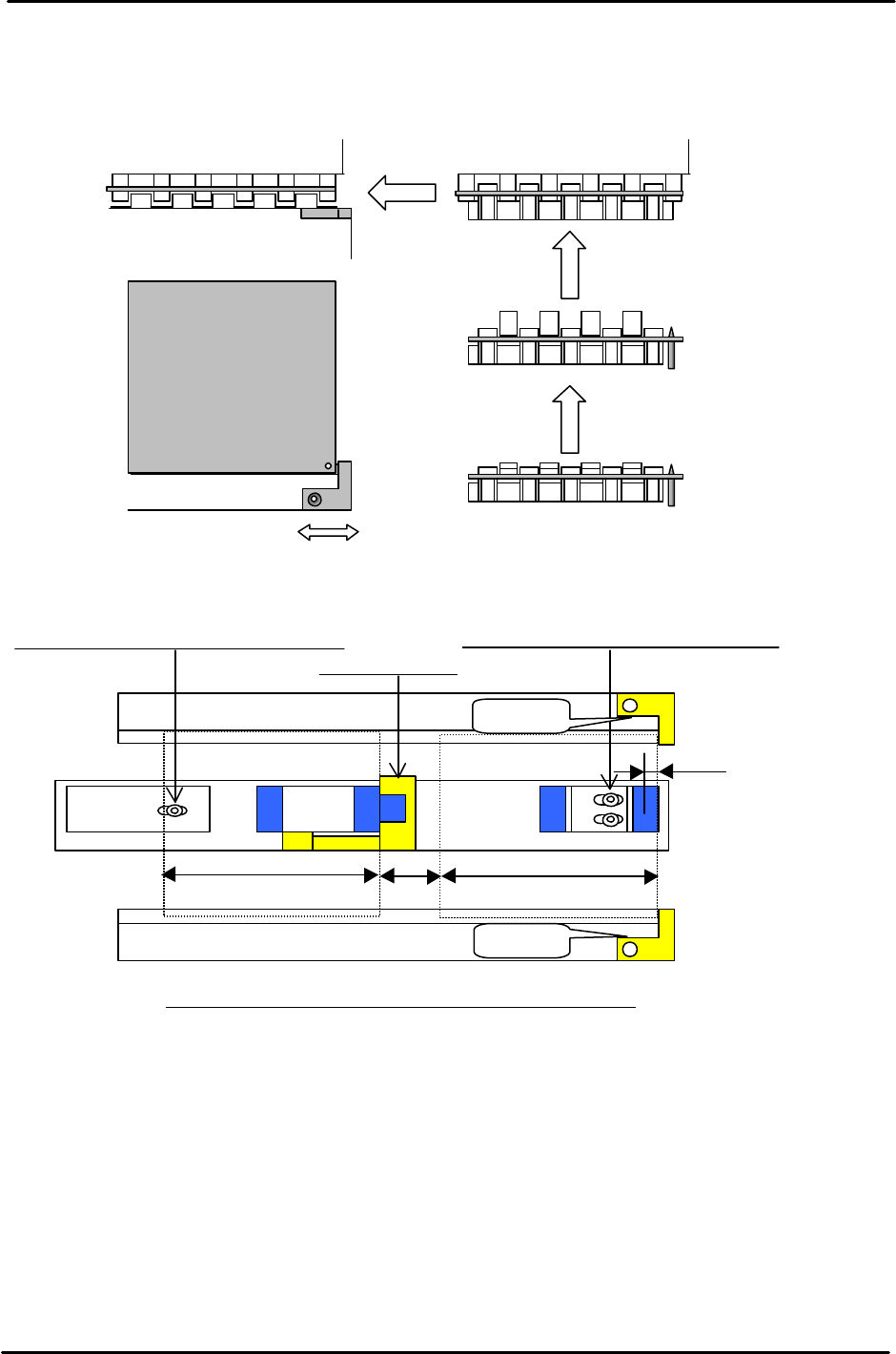
5.22 PCB Stopper and Check Sensor Adjustment
<<IN Conveyor (Fixed) Stopper Installation>>
Install the stoppers and adjust the sensors for 2-PCB-loading, using the maximum length
board: (CP-643E: 220MM)
Install the stoppers only after the X, Y, and Z, axes, “Loading Position” has been calibrated.
1. With the first PCB stoppers from the In conveyor removed, move the XY table to the IN
loading position. (DO NOT raise the Z-axis) The 1
st
PCB moveable stopper should be
down. (Turn On “Y079” to lower the 1
st
PCB stopper)
2. Turn ON “Y051”, (Main clamp open), and position the maximum length board (for 2
PCB’s) on the reference and secondary pins. Turn ON “Y050” (Main clamp close), and
clamp the PCB.
3. Turn ON “Y072”, (In carrier close) , “Y074”, (In carrier advance) ,and “Y073”, (In carrier
open). Manually raise the Z to the IN loading position.
4. Turn ON “Y072” (In carrier close), and “Y044”(Main clamp open), and lower Z to the “Z0”
position. (The PCB should now be clamped on the carrier.)
5. Turn ON “Y075”(In carrier retract), “Y076” (In lifter up), and “Y073B” (In carrier open),
“Y077” (In lifter down), “Y072” (In carrier close), and “Y074” (In carrier advance). (the
PCB is now loaded at the correct position on the IN conveyor.) See Fig. 32.
6. Set the first PCB stoppers against the leading edge of the PCB. (be careful not to move
the board)
7. Loosen the sensor positioning bolt for the first PCB check sensor and position the sensor
5mm from the leading edge of the first PCB. See Fig. 33.
FK-9F98-05 CP-643E Training Text for Service Engineers
Edition 5.0 Chapter 5. Loader and Conveyor Adjustment [21/28]
Fuji Machine Mfg. Co., Ltd. Okazaki
SMT Equipment Quality Assurance Dept.
Technical Support Div. Section No.2
5-
21
8. Set the IN PCB clearance check sensor switch to “D_ON”, and both the arrival and speed
reduction sensor switches to “L_ON”.
Figure 32
Figure 33
5mm
15mm
(220mm)
(2
nd
PCB)
No Gap
No Gap
2
nd
PCB Stopper
(220mm)
(1
st
PCB)
1
st
PCB Stopper
1
st
PCB Stopper
Sensor positioning bolt for the 1
st
PCB
Sensor positioning bolt for the 2
nd
PCB
Stopper and Sensor Position
ing
for the IN conveyor.
FK-9F98-05 CP-643E Training Text for Service Engineers
Edition 5.0 Chapter 5. Loader and Conveyor Adjustment [22/28]
Fuji Machine Mfg. Co., Ltd. Okazaki
SMT Equipment Quality Assurance Dept.
Technical Support Div. Section No.2
5-
22
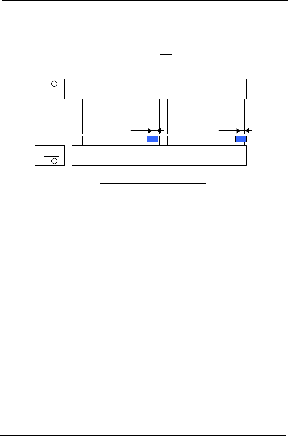
<<IN Carrier Sensor Adjustment>>
1. Load two PCBs on the IN carrier. “X0B1” (In carrier 1 detection check), “X0B2” (IN carrier 2
detection check) shall come ON when “Y074”, (In carrier advance) is ON. Adjust the sensor
position 5mm from the leading edge of each board. Ensure that the sensor switch is set to
“L_ON”. And make sure that the volume is at MAX position.
(1
st
PCB)
5mm
(2
nd
PCB)
5mm
IN Carrier
Sensor Positioning for the IN Carrier
Figure 34