IPC-TM-650 EN 2022 试验方法--.pdf - 第219页
1 Scope The purpose of this test me thod is to measure the thickness and phosphorous (P) concentration of chemically (electroless) deposited nickel (Ni) coatings by ( energy disper- sive) X-ray fluorescence ( XRF) analys…
1 Scope
This test method is used to determine the ability of
a solder mask to resist degradation by solvents and cleaning
agents.
2 Applicable Documents
Qualification and Performance of Permanent
Solder Mask
Multipurpose One-Sided Test Pattern
3 Test Specimens
Six (6) IPC-B-25A boards coated with
solder mask on the top side. Five are to be tested and one is
to be held as a control.
The IPC-A-25A-G-KIT artwork package provides the Gerber
files necessary for the fabrication of the standard IPC-B-25A
test board used with this test method.
4 Apparatus and Reagents
4.1
Reagent Grade 2-Propanol (Isopropyl Alcohol)
4.2
Deionized Water (DI Water) with resistivity ≥2 MΩ-cm
and ≤10 MΩ-cm
4.3
10% Alkaline Detergent [by volume], which shall be
comprised of
• 5% alkanolamine
• 2.5% 2-butoxyethanol
• 2.5% glycol ether
• 90% DI Water
4.4
Monoethanolamine
4.5
Miscellaneous laboratory-ware (e.g., beakers, funnels,
storage bottles, graduated cylinders) including:
1) A hot plate capable of heating up to 65 °C [149 °F]
2) A thermometer capable of measuring accurately up to 100
°C [212 °F]
3) A vent hood, or performed with adequate ventilation
4.6
Thermometer with measurement uncertainty less than 2
°C [3.6 °F] and precision better than 1 °C [1.8 °F].
5 Procedures
5.1 Chemical Exposure
5.1.1
Prepare the solvents and cleaning agents as outlined
in Section 4 and Table 1.
5.1.2
Completely immerse one test specimen in each of the
solutions shown in Table 1. A new specimen is to be used for
each chemical.
5.1.3
After immersion, hang the specimens to dry for ten
minutes at ambient laboratory conditions.
5.2 Visual Examination
5.2.1
Visually examine each printed board with corrected
20/20 vision without magnification for delamination or surface
degradation such as cracks, tackiness, blisters or swelling of
the solder mask.
6 Notes
6.1 Safety
Operator should be trained and familiar with the
hazards inherent to the chemicals being used and analyzed.
Proper personal safety equipment, such as safety glasses,
gloves and splash apron, and adequate ventilation shall be
used.
1. www.ipc.org/onlinestore
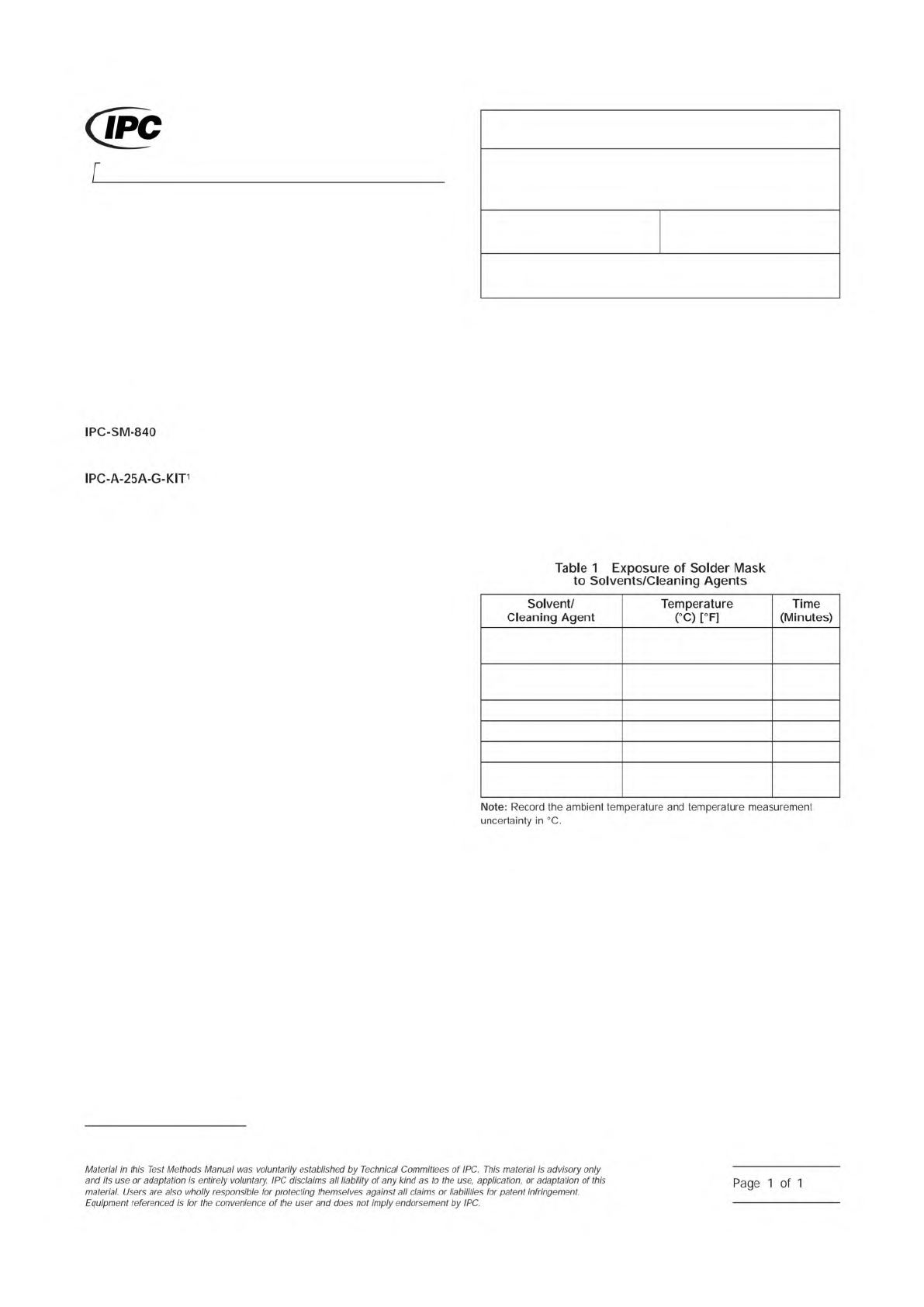
Isopropanol
Ambient
Laboratory Conditions
2
75% isopropanol/
25% deionized water
46 ± 2 °C [115 ± 3.6 °F] 15
10% Alkaline detergent 57 ± 2 °C [135 ± °F] 2
Monoethanolamine 57 ± 2 °C [135 ± °F] 2
Deionized water 60 ± 2 °C [140 ± °F] 5
D-Limonene
Ambient
Laboratory Conditions
2
3000 Lakeside Drive, Suite 309S
Bannockburn, IL 60015-1219
IPC-TM-650
TEST METHODS MANUAL
Number
2.3.42
Subject
Solder Mask - Resistance to Solvents and
Cleaning Agents
Date
03/07
Revision
Originating Task Group
Solder Mask Performance Task Group (5-33b)
ASSOCIATION CONNECTING
ELECTRONICS INDUSTRIES
®
IPC-SM-840
IPC-A-25A-G-KIT1
Table
1
Exposure
of
Solder
Mask
to
Solvents/Cleaning
Agents
Solvent/
Cleaning
Agent
Temperature
(
℃)
[°F]
Time
(Minutes)
Note:
Record
the
ambient
temperature
and
temperature
measurement
uncertainty
in
℃
.
Material
/n
this
Test
Methods
Manual
was
voluntarily
established
by
Technical
Committees
of
I
PC.
This
material
/s
advisory
only
and
"s
use
or
adaptation
,
s
entirely
voluntary.
IPC
disclaims
all
liability
of
any
kind
as
to
the
use,
application,
or
adaptation
of
this
material.
Users
are
also
wholly
responsible
for
protecting
themselves
against
all
claims
or
liabilities
for
patent
infringement.
Equipment
referenced
/s
for
the
convenience
of
the
user
and
does
not
imply
endorsement
by
IPC.
Page
1
of
1
1 Scope
The purpose of this test method is to measure the
thickness and phosphorous (P) concentration of chemically
(electroless) deposited nickel (Ni) coatings by (energy disper-
sive) X-ray fluorescence (XRF) analysis.
The measurement is nondestructive and noncontact, and can
be performed either in ambient atmosphere or under vacuum.
Measurements
be made on a defined feature (equi-
valent to a typical SMT pad) of 1.5 mm x 1.5 mm [0.060 in x
0.060 in] or equivalent area, using a 0.6 mm diameter collima-
tor. This equates to a measuring spot size (analysis area) of
1 mm diameter.
This test method is designed primarily for failure analysis, pro-
cess qualification and process auditing. It is not intended for
daily production control, due to the complexity and cost of the
equipment required.
2 Applicable Documents
Specification for Electroless Nickel/Electroless
Palladium/Immersion Gold (ENEPIG) Plating for Printed Circuit
Boards
Specification for Electroless Nickel/Immersion
Gold (ENIG) Plating for Printed Circuit Boards
3 Test Specimen
This test method is primarily designed
for measurement of the phosphorus content in ‘‘as plated’’
ENIG PWBs. Other ENIG or electroless nickel (EN) plated sub-
strate materials may also be tested using this method, includ-
ing flexible circuits, silicon wafers, aluminum or steel. The typi-
cal thickness range of the NiP layer on PWB substrates is 3 to
6 µm [118.1 to 236.2 µin]. The Phosphorous content can
range from 0 % to 14% by weight. Minimum and maximum
thickness for single layers of electroless nickel required for
accurate determination of the P content is 0.5 µm to 25 µm
[19.7 µin to 984 µin]. The maximum thickness of gold present
on the surface of the specimen when tested
be less
than 0.10 µm [0.004 µin]. For samples with thicker gold, the
gold must be removed by chemical stripping or Ion milling
prior to evaluation.
While this test method is also suitable for evaluating phospho-
rus content in ENEPIG samples, the thickness of both the
gold (Au) and palladium (Pd) layers needs to be considered.
The maximum thicknesses of the layers over the electroless
nickel on ENEPIG specimens when tested
exceed
0.05 µm [0.002 µin] of Au and 0.10 µm [0.004 µin] of Pd on
top of the EN layer. This constraint will impact measurement
of ENEPIG samples plated on the higher side of the current
IPC-4556 specification. For samples with gold thicknesses
above 0.05 µm [0.002 µin], chemical or Ion milling stripping
may be carried out prior to evaluation. With the gold removed,
the maximum thickness of palladium on a specimen when
tested
be 0.25 µm [0.0098 µin].
Electroless palladium deposits may also contain phos-
phorus and its contribution to the total phosphorus content
must be taken into account when reporting the phosphorus
content of the deposit.
The sample to be tested should be flat and ideally not popu-
lated with components in the area of measurement. If testing
is done on populated boards, consideration has to be given to
measurement location, such that none of the electronic com-
ponents block the fluorescent radiation from reaching the
detector, as described in Section 5.4.
The test specimen requires no other sample preparation.
4 Apparatus
An X-ray fluorescence spectrometer consist-
ing of the following:
• A radiation source (X-ray tube with adjustable HV power
supply from 10 kV to 50 kV).
• A primary beam filter and safety shutter assembly.
• A video camera.
• An X-ray collimator or a polycapillary X-ray optic.
• An energy dispersive Silicon Drift Detector SDD (a device in
which charge carriers created by the incidence of X-ray pho-
tons on a high purity silicon substrate are directed to a mea-
suring electrode by an applied transverse electric field),
including electronics.
• Evaluation software capable of simultaneously measuring
coating thickness and composition of multiple layers. The
software of the instrument
have the capability of mul-
tiple excitation modes. It is necessary to apply different exci-
tation conditions; a soft excitation for the excitation of P-K at
10 kV and a hard excitation for Ni-K at 50 kV.
• A programmable X-Y positioning stage (accurate positioning
is required especially if small areas are to be analyzed).
• The instrument must be able to record the Intensities of the
individual radiation components of the Phosphorous K
energy line (I
P-K
) and the Nickel K energy line (I
Ni-K
) with suf-
ficient precision.
3000 Lakeside Drive, Suite 105N
Bannockburn, IL 60015-1249
IPC-TM-650
TEST METHODS MANUAL
Number
2.3.44
Subject
Determination of Thickness and Phosphorus
Content in Electroless Nickel (EN) Layers by X-Ray
Fluorescence (XRF) Spectrometry
Date
03/16
Revision
Originating Task Group
Plating Processes Subcommittee (4-14)
Association
Connecting
Electronics
Industries
shall
shall
Note:
IPC-4556
IPC-4552
shall
shall
shall
not
Material
in
this
Test
Methods
Manual
was
voluntarily
established
by
Technical
Committees
of
I
PC.
This
material
is
advisory
only
and
"s
use
or
adaptation
is
entirely
voluntary.
IPC
disclaims
all
liability
of
any
kind
as
to
the
use,
application,
or
adaptation
of
this
material.
Users
are
also
wholly
responsible
for
protecting
themselves
against
all
claims
or
liabilities
for
patent
infringement.
Equipment
referenced
/s
for
the
convenience
of
the
user
and
does
not
imply
endorsement
by
IPC.
Page
1
of
4
A Certified Reference Material (CRM) covering the measuring
range of the application as described in 5.2.
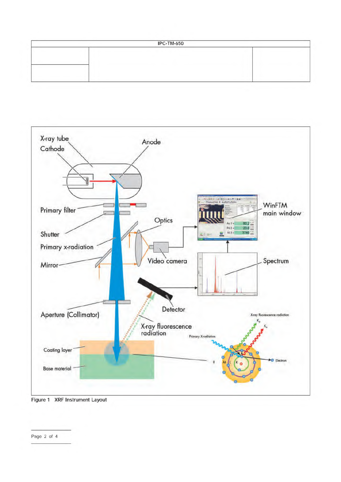
A typical instrument layout is shown in Figure 1.
IPC-2344-1
Number
2.3.44
Subject
Determination of Thickness and Phosphorus Content in
Electroless Nickel (EN) Layers by X-Ray Fluorescence (XRF)
Spectrometry
Date
03/16
Revision
IPC-TM-650
—
Anode
Primary
filter
Shutter
3749
Primary
x-radiation
Spectrum
Mirror
Detector
Aperture
(Collimator)
Primary
X-rodiation
Coating
laye
Electron
Base
material
X-ray
tube
Cathode
Video
camera
X<ay
fluorescence
radiation
WinFTM
main
window
Figure
1
XRF
Instrument
Layout
Page
2
of
4