IPC-TM-650 EN 2022 试验方法--.pdf - 第604页
photolithographic processes such that a minimum of twelve good specimens are yielded at the end of 3.4.5. On the ‘ ‘Test Surface,’’ etch f our conductors 3 .2 m m [0.126 in] w ide, 5.7 mm [0.224 in] pitch, 230 - 250 mm […
[ [
[
Note:
IPC-TM-650
Number
Subject Date
Revision
Page 2 of 3
2.5.17.2
Volume
Resistivity
of
Conductive
Materials
Used
in
High
Density
Interconnection
(HDI)
and
Microvias,
Two-Wire
Method
11/98
3.1
Conductor
Any
high
resistance
conductor
used
in
HDI
applications
(polymer
thick
film,
via
fill,
metal,
metal
compos¬
ites,
transient
liquid
phase
sintering,
organometallic,
conduc¬
tive
polymer,
etc.).
Copper
foils
used
in
HDI
should
be
tested
according
to
IPC-TM-650,
Method
2.5.14.
3.2
Substrate
Unless
otherwise
specified,
the
substrate
shall
be
a
PCB
laminate,
etched
to
remove
all
copper.
Other
acceptable
substrates
(when
specified)
may
be
plate
glass,
insulated
metals,
or
flexible
circuit
base
material.
3.3
Screen
For
materials
that
are
screen
printed,
unless
otherwise
specified,
the
screen
shall
be
as
outlined
in
3.3.1
through
3.3.3.
3.3.1
Type
200
mesh,
stainless
steel,
35
pm
wire
3.3.2
Emulsion
<15
pm
emulsion
build
up
3.3.3
Wire
Angle
22.5°
to
45°
3.4
Typical
Patterns
3.4.1
Pattern
Serpentine
with
0.5
mm
wide
lines
and
spaces
and
200
to
1000
long
(10
cm
to
50
cm).
The
larger
the
number
of
squares,
the
higher
the
resistance
and
more
accurate
the
measurement.
3.4.2
Print
1
.25
mm
snapoff
0.2
Kg
to
1
.0
Kg
squeegee
pressure
per
cm
squeegee
length
2.5
cm/sec.
to
12.5
cm/sec.
draw
speed
3.5
Cure
Conditions
The
conductor
shall
be
cured
according
to
the
manufacturer's
specifications.
Parts
are
allowed
to
cool
to
room
temperature,
after
which
they
are
measured
for
resistance.
4
Equipment/Apparatus
4.1
A
digital
multimeter
capable
of
resolving
0.1
Q
resis¬
tance
is
required.
This
unit
must
be
accurately
calibrated.
An
example
would
be
a
Fluke
70
series
digital
multimeter.
For
improved
accuracy
in
this
measurement,
a
larger
number
of
and/or
a
more
sensitive
multimeter
can
be
utilized.
4.2
A
screen
printer
capable
of
making
0.5
mm
line/space
circuitry,
or
any
other
method
for
preparing
the
desired
circuit
pattern
4.3
Equipment
to
measure
the
test
circuit
conductor
length,
width,
and
thickness.
If
the
number
of
squares
is
accurately
known
(length/width
of
circuit)
from
the
artwork
and
standard
process
conditions,
then
only
the
thickness
needs
to
be
mea¬
sured
on
each
specimen.
Thickness
can
be
determined
by
various
methods:
cross-section/optical
microscopy,
profilo¬
meter
measurement,
or
calculation
from
deposition
weight
and
material
density.
If
the
circuit
thickness
is
very
uniform,
then
optical
sectioning
is
the
preferred
method
for
obtaining
the
thickness.
If
the
circuit
thickness
is
thought
to
be
non-
uniform,
thickness
may
then
be
determined
by
averaging
pro¬
filometer
readings
or
determining
average
thickness
from
the
weight
of
the
material
deposited
(knowing
the
length,
width,
and
density
that
the
thickness
can
be
determined).
5
Procedure
5.1
Samples
Prepare
a
minimum
of
five
test
specimens
according
to
3.1
through
3.5.
5.2
Conditioning
Condition
the
specimens
at
23℃
土
5
℃,
50%
RH
(±
5%)
for
24
hours.
5.3
Measurement
5.3.1
Measure
the
circuit
length,
width,
and
thickness
using
the
equipment
described
in
4.3.
5.3.2
Apply
the
digital
multimeter
leads
to
the
pads
at
each
end
of
the
circuit.
Measure
and
record
the
resistance
in
ohms.
For
a
resistance
less
than
2
Q,
see
6.1.
5.3.3
Measure
the
resistance
of
a
minimum
of
five
speci¬
mens
and
average
the
values.
5.4
Calculation
Calculate
the
volume
resistivity
for
each
specimen
from
the
equation
below:
where:
R
=
average
resistance
of
a
single
specimen
in
ohms
t
二
thickness
of
the
conductive
specimen
in
cm
L
=
length
conductive
specimen
in
cm
W
=
width
conductive
specimen
in
cm
The
ratio
L/W
is
the
number
of
squares.
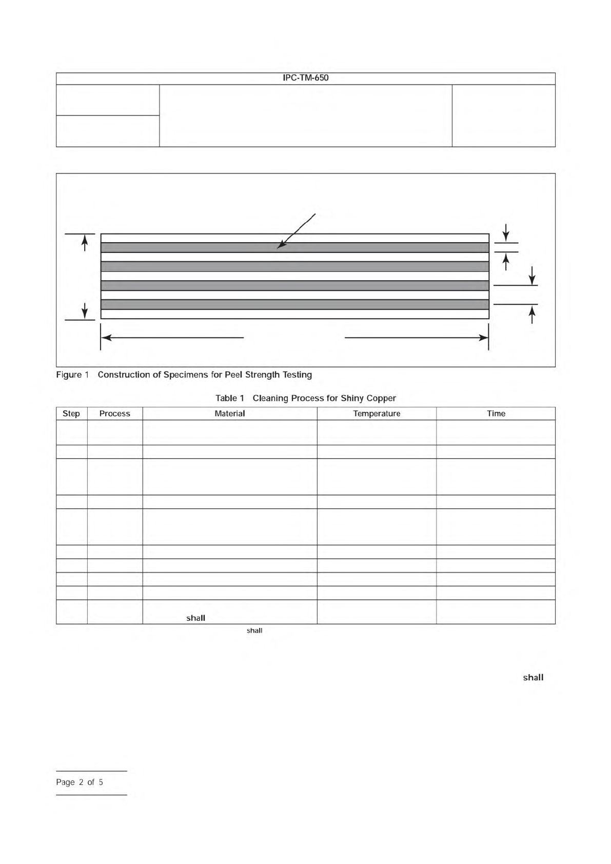
photolithographic processes such that a minimum of twelve
good specimens are yielded at the end of 3.4.5. On the ‘‘Test
Surface,’’ etch four conductors 3.2 mm [0.126 in] wide,
5.7 mm [0.224 in] pitch, 230 - 250 mm [9 - 10 in] long on a
nominal 25 mm [1 in] wide strip of flexible base dielectric (see
Figures 1 and 2).
3.4 Conditioning and Aging Procedure
3.4.1
Twelve specimens, as described in section 3, be
subjected to a stabilization period of a minimum of 24 hours
at 23 °C ± 2 °C [73.4 °F ± 3.6 °F] and 50% ± 5% RH.
IPC-2-6-21a
Metal Conductor (4 each)
3.2 mm
[0.126 in]
25 mm [1 in]
(nom.)
230–250 mm [9–10 in]
5.7 mm
[0.224 in]
1 Soak Clean
Use commercially available acid or alkaline
cleaners
Per supplier recommended
temperature
Per supplier recommended
time
2 Rinse Running tap water Room Temperature 3 - 5 minutes
3 Microetch
Sodium persulfate: Two liters of deionized
water, 280 grams of sodium persulfate,
25 cc sulfuric acid
Room Temperature 1 - 2 minutes
4 Rinse Running tap water Room Temperature 1 minute
5 Acid Dip
Sulfuric acid 10% by volume, dilution 1.8
liters deionized water, 200 cc sulfuric acid
96% assay
Room Temperature 45 seconds
6 Rinse Running tap water Room Temperature 1 minute
7 Rinse Deionized water Room Temperature 1 minute
8 Dry Force air dry or blot with paper towels Room Temperature 1 - 3 minutes
9 Bake Bake in clean air-circulating oven 110 ± 5 °C [230.0 ± 9.0 °F] 10 to 15 minutes
10 Lamination
*Maximum delay between bake and
lamination
be 30 minutes
*Lamination conditions (e.g., pressure, temperature, time, etc.) conform to suppliers’ recommendations.
Number
2.6.21
Subject
Service Temperature of Metal-Clad Flexible Laminate, Cover
Material and Adhesive Bonding Films
Date
6/11
Revision
B
IPC-TM-650
—
Figure
1
Construction
of
Specimens
for
Peel
Strength
Testing
Table
1
Cleaning
Process
for
Shiny
Copper
shall
Step
Process
Material
Temperature
Time
shall
shall
Page
2
of
5
3.4.2
Measure the flexible base dielectric thickness and the
metal thickness of the twelve specimens by micrometer, cali-
per or similar following the stabilization period in 3.4.1. Nomi-
nal metal thickness to be tested is either 1 oz or 34.3 µm
[1350 µin] thick (preferred) or
1
⁄
2
oz or 17.1 µm [680 µin] thick.
3.4.3
On the specimens stabilized in 3.4.1, measure and
verify that the conductor widths are 3.2 mm ± 0.15 mm
[0.126 in ± 5.9 µin].
3.4.4
Examine the twelve specimens measured in 3.4.3
using normal or corrected 20/20 (also termed 6/6 or 1.0)
vision, and discard any peel strips showing the presence of
any wrinkles, cracks, blisters, or loose conductors. Twelve
specimens are required for the test, so any specimens not
meeting this criterion
be replaced.
3.4.5
Per IPC-TM-650, TM 2.4.13, Method B, subject the
specimens examined in 3.4.4 to pre-drying and then solder
float.
3.4.6
Examine the specimens subjected to solder float in
3.4.5 using normal or corrected 20/20 (also termed 6/6 or 1.0)
vision. Discard any peel strips showing the presence of any
wrinkles, cracks, blisters, or loose conductors. Verify that at
least twelve good specimens remain.
3.4.7
Place six specimens into an air-circulating oven at the
desired Service Temperature value. The oven temperature
be held at a tolerance of ± 3°C [5.4 °F]. The specimens
are to continuously remain in the oven for 1000 hours, -0
hours / +12 hours.
3.4.8
After being aged per 3.4.7, the test specimens
be cooled to room temperature at standard ambient labora-
tory conditions. After being cooled to room temperature, the
thermally aged (oven conditioned) specimens
be sub-
jected to a stabilization period of a minimum of 24 hours at
23 °C ± 2 °C [73.4 °F ± 3.6 °F] and 50% ± 5% RH.
3.4.9
After the stabilization period in 3.4.8, examine the
specimens using normal or corrected 20/20 (also termed 6/6
or 1.0) vision, and record the presence of any wrinkles,
cracks, blisters, or loose conductors, or any delamination.
3.5 Measurement of Peel Strength
3.5.1
AABUS, test specimens may have rigid reinforcement
material attached to all twelve specimens that were subjected
to the solder float in 3.4.5, including those six specimens that
were additionally subjected to thermal aging in 3.4.7. The rigid
reinforcement material
be attached prior to condi-
tioning and aging. The attachment of the rigid reinforcement
material depends on a number of factors, including the type of
peel test apparatus as described in IPC-TM-650, Method
2.4.9. If the rigid reinforcement material is to be utilized, it
should be adhered to the specimens using double-faced
adhesive tape or appropriate adhesive system to the back
side of the specimens.
If the test specimens are generated from double-clad flexible
base materials with metal remaining on the non-test side, the
additional rigid reinforcement material is unnecessary and
should not be used.
3.5.2
Measure the peel strength of the twelve conductors
per the procedures outlined in IPC TM-650, Method 2.4.9.
Specifically, peel the etched copper conductors away from
the dielectric at a 90° angle and at a 50.8 mm [2 in] per min-
ute crosshead speed.
3.6 Document and Report Results
3.6.1
Calculate the average peel strength of the six speci-
mens that were only exposed to the solder float (i.e., only as
per 3.4.5 and
exposed to the thermal aging of 3.4.7). Do
the same for the six thermally aged specimens per 3.4.7. Cal-
culate the ratio of the ‘‘thermally aged’’ average peel
strengths divided by the solder-floated only average peel
strength to determine the percentage retention of peel
strength. Record this number to ± 1% accuracy.
[Ave. of Six (6) Peel Strengths of Thermally Aged Specimens]
[Ave. of Six (6) Peel Strengths of Solder Floated-Only Specimens
x 100 = % of Peel Strength Retained
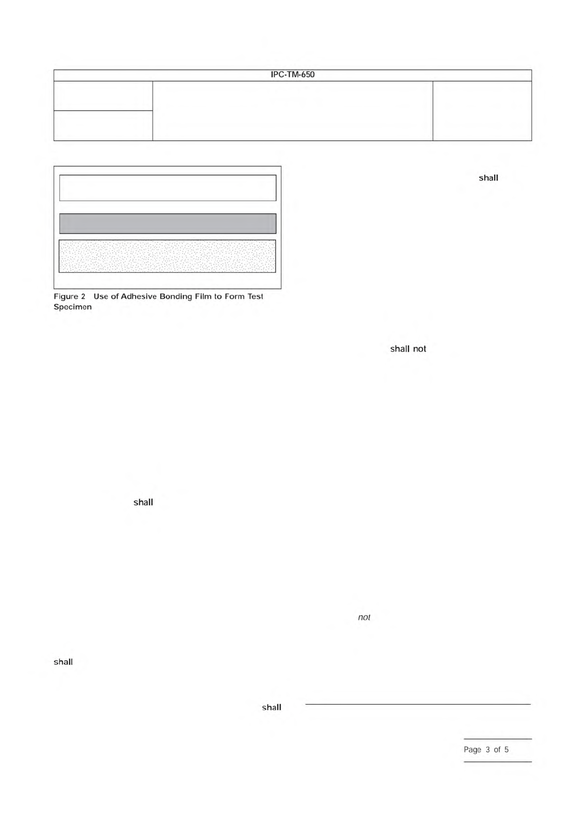
IPC-2-6-21-2
1 oz ED or RA Copper Foil Test Surface
(Shiny side toward the adhesive)
1 oz ED Copper Foil with Treated Matte
Side Inward as Support Material
Adhesive Bonding Film
Number
2.6.21
Subject
Service Temperature of Metal-Clad Flexible Laminate, Cover
Material and Adhesive Bonding Films
Date
6/11
Revision
B
IPC-TM-650
Figure
2
Use
of
Adhesive
Bonding
Film
to
Form
Test
Specimen
shall
not
shall
shall
shall
Page
3
of
5