IPC-TM-650 EN 2022 试验方法--.pdf - 第676页
NOTE: NO T E : No. Pattern Resistance (Ohms) Lo gOhms IPC-TM-650 Page 4 of 4 Number 2.6.3.5 Subject Bare Board Cleanliness by Surface Insulation Resistance Date 01/04 Revision 3.98E+11 = 3.98 x 10¹¹ In many spreadsheet s…
IPC-TM-650
Page 3 of 4
Number
2.6.3.5
Subject
Bare
Board
Cleanliness
by
Surface
Insulation
Resistance
Date
01/04
Revision
After
96
hours
total,
repeat
the
measurement
series.
Regard¬
less
of
the
outcome
of
the
measurements,
the
test
terminates
after
this
measurement
series.
5.6
Data
Analysis
The
average
insulation
resistance
(IRavg)
is
calculated
as
follows:
IRavg
=
1
°
•
N
•
N
£iogio(iR>
1
Where:
N
=
Number
of
Test
Points
(32
nominal
for
each
set
of
eight
patterns)
IRi
=
individual
insulation
resistance
measurements
See
6.4
for
an
example
No
individual
insulation
resistance
value
may
be
more
than
a
factor
of
1
0
below
the
specified
minimum
value.
Where
an
assignable
cause
of
low
insulation
resistance,
which
is
properly
attributable
to
the
laminate
itself,
or
to
the
process
used
to
produce
the
PWB,
can
be
found,
then
such
a
value
can
be
excluded
from
calculating
the
average
value,
provided
that
at
least
30
test
points
are
included
in
the
average.
Such
assignable
causes
include
the
following:
•
Contamination
on
the
insulating
surface
of
the
board,
such
as
lint,
solder
splines
or
water
droplets
from
the
chamber.
•
Incompletely
etched
patterns
that
decrease
the
insulating
space
between
the
conductors
by
more
than
the
amount
allowed
in
the
appropriate
design
requirements
drawing.
•
Scratched,
cracked,
or
obviously
damaged
insulation
between
conductors.
6
Notes
6.1
If
condensation
occurs
on
the
test
specimens
in
the
environmental
chamber
while
the
samples
are
under
voltage,
dendritic
growth
will
occur.
This
can
be
caused
by
a
lack
of
sufficient
control
of
the
humidification
of
the
oven.
Water
spot¬
ting
may
also
be
observed
in
some
ovens
where
the
airflow
in
the
chamber
is
from
back
to
front.
In
this
case,
water
conden¬
sation
on
the
cooler
oven
window
can
be
blown
around
the
oven
as
microdroplets
which
deposit
on
test
specimens
and
cause
dendritic
growth
if
the
spots
bridge
the
distance
between
two
electrified
conductors.
Both
of
these
conditions
must
be
eliminated
for
proper
testing.
6.2
Tight
control
of
the
test
humidity
is
critical
for
this
test
method.
A
difference
of
5%
relative
humidity
can
result
in
a
0.5
-
1
.0
decade
difference
in
the
measured
resistance.
The
uniformity
of
the
environment
is
also
important.
A
fully
loaded
chamber,
where
airflow
is
severely
impeded,
may
have
a
30-40%
RH
range
within
the
chamber
workspace.
6.3
The
polarity
of
the
applied
voltage
is
not
important
as
long
as
the
application
is
consistent
(e.g.,
Pads
1,
3,
5
are
positive
and
2,
4
are
at
opposite
potential,
vs.
Pads
2
and
4
positive,
and
Pads
1
,
3,
5
at
opposite
potential).
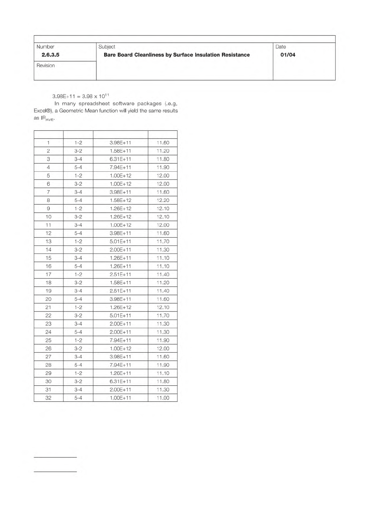
6.4
Example
of
Numerical
Calculations
Eight
5-point
test
patterns
(4
measurements
each)
LogOhms
二
base-
10
logarithm
of
measured
resistance
Average
of
LogOhms
=
11
.62
IRave
二
Antilog
(1
1
.62)
=
4.19E+1
1
ohms
IRave
二
Geometric
Mean
NOTE:
NOTE:
No. Pattern Resistance (Ohms) LogOhms
IPC-TM-650
Page 4 of 4
Number
2.6.3.5
Subject
Bare
Board
Cleanliness
by
Surface
Insulation
Resistance
Date
01/04
Revision
3.98E+11
=
3.98
x
1011
In
many
spreadsheet
software
packages
(.e.g,
Excel®),
a
Geometric
Mean
function
will
yield
the
same
results
1
1-2
3.98E+11
11.60
2
3-2
1
.58E+1
1
11.20
3
3-4
6.31
E+11
11.80
4
5-4
7.94E+11
11.90
5
1-2
1.00E+12
12.00
6
3-2
1.00E+12
12.00
7
3-4
3.98E+11
11.60
8
5-4
1.58E+12
12.20
9
1-2
1.26E+12
12.10
10
3-2
1.26E+12
12.10
11
3-4
1.00E+12
12.00
12
5-4
3.98E+1
1
11.60
13
1-2
5.01
E+11
11.70
14
3-2
2.00E+11
11.30
15
3-4
1.26E+11
11.10
16
5-4
1.26E+11
11.10
17
1-2
2.51
E+11
11.40
18
3-2
1
.58E+1
1
11.20
19
3-4
2.51
E+11
11.40
20
5-4
3.98E+1
1
11.60
21
1-2
1.26E+12
12.10
22
3-2
5.01
E+11
11.70
23
3-4
2.00E+1
1
11.30
24
5-4
2.00E+11
11.30
25
1-2
7.94E+11
11.90
26
3-2
1.00E+12
12.00
27
3-4
3.98E+11
11.60
28
5-4
7.94E+11
11.90
29
1-2
1.26E+11
11.10
30
3-2
6.31
E+11
11.80
31
3-4
2.00E+11
11.30
32
5-4
1
.00E+1
1
11.00
IPC-J-STD-004
IPC-A-600
GR-78-CORE
ASTM D-257
IPC-A-25A
IPC-A-50
Figure 1
Figure 2
Material in this Test Methods Manual was voluntarily established by Technical Committees of IPC. This material is advisory only
and its use or adaptation is entirely voluntary. IPC disclaims all liability of any kind as to the use, application, or adaptation of this
material. Users are also wholly responsible for protecting themselves against all claims or liabilities for patent infringement.
Equipment referenced is for the convenience of the user and does not imply endorsement by IPC.
Page 1 of 3
r
ASSOCIATION
CONNECTING
/
ELECTRONICS
INDUSTRIES
®
221
5
Sanders
Road
Northbrook,
IL
60062-6135
IPC-TM-650
TEST
METHODS
MANUAL
1
Scope
This
test
method
is
used
to
characterize
the
effects
of
flux
residues
on
electrical
performance
by
determin¬
ing
the
degradation
of
electrical
insulation
resistance
under
conditions
of
high
temperature
and
humidity.
This
method,
in
conjunction
with
the
supporting
documenta¬
tion
in
IPC-J-STD-004,
is
intended
to
be
equivalent
to
Telcor¬
dia
Technologies
GR-78-CORE,
Section
13.1,
(Corrosiveness
of
Soldering
Fluxes)
and
is
used
primarily
by
telecommunica¬
tions
companies
to
qualify
the
candidate
flux
or
solder
paste.
2
Applicable
Documents
Requirements
for
Soldering
Fluxes
Acceptability
of
Printed
Board
Physical
Design
and
Manufacture
of
Telecom¬
munications
Product
-
Telcordia
Technologies
(Formerly
Bellcore)
Standard
Test
Methods
for
DC
Resistance
or
Conductance
of
Insulating
Materials
2.1
Master
Drawings
Telcordia
Technologies
Test
Pattern
(GR-78-CORE,
Figures
14.1
and
14.2)
Multipurpose
1
-sided
Test
Pattern
Surface
Insulation
Resistance
Phoenix
Board
3
Test
Specimens
The
test
specimens
for
this
test
method
may
be
either
of
the
interdigitated
comb
pattern
shown
in
Fig¬
ures
1
or
2.
These
test
patterns
can
be
produced
in
a
number
of
formats.
Both
of
these
patterns
can
be
found
on
the
IPC-B-50
Stan¬
dard
Test
Board.
The
pattern
shown
in
Figure
2
can
be
found
on
the
IPC-B-25A
test
board
(pattern
D).
Artwork
for
manu¬
facturing
these
boards
is
available
through
the
master
draw¬
ings
listed
in
2.1.
Contact
IPG
for
a
listing
of
vendors
provid¬
ing
prefabricated
test
boards.
The
comb
pattern
in
Figure
1
has
0.65
mm
[0.025
in]
lines
and
1
.27
mm
[0.050
in]
spacings.
This
test
pattern
is
also
com¬
monly
referred
to
as
the
Bellcore
pattern.
The
comb
pattern
in
Figure
2
has
0.32
mm
[0.0125
in]
lines
and
spaces
(see
Note
6.4).
Number
2.6.3.6
Subject
Surface
Insulation
Resistance
-
Fluxes
-
Telecommunications
Date
Revision
01/04
Originating
Task
Group
Surface
Insulation
Resistance
Task
Group,
5-32b