IPC-TM-650 EN 2022 试验方法--.pdf - 第525页
3. 1 . 7 G e ne r al T h ie vi n g T hi ev i n g w hi c h i s t h e u se o f no nt erm in at ed c op per s tr uc tu res , s uc h as p la n es, p ad s, and/or c on ductors adjacent t o test lines that ensure pl ating cons…
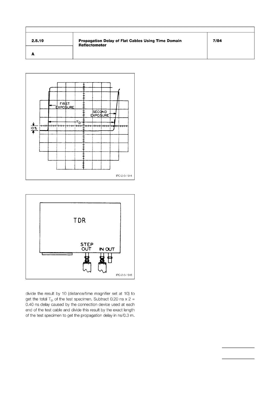
Figure 5 Dual Exposure Picture TDR Trace
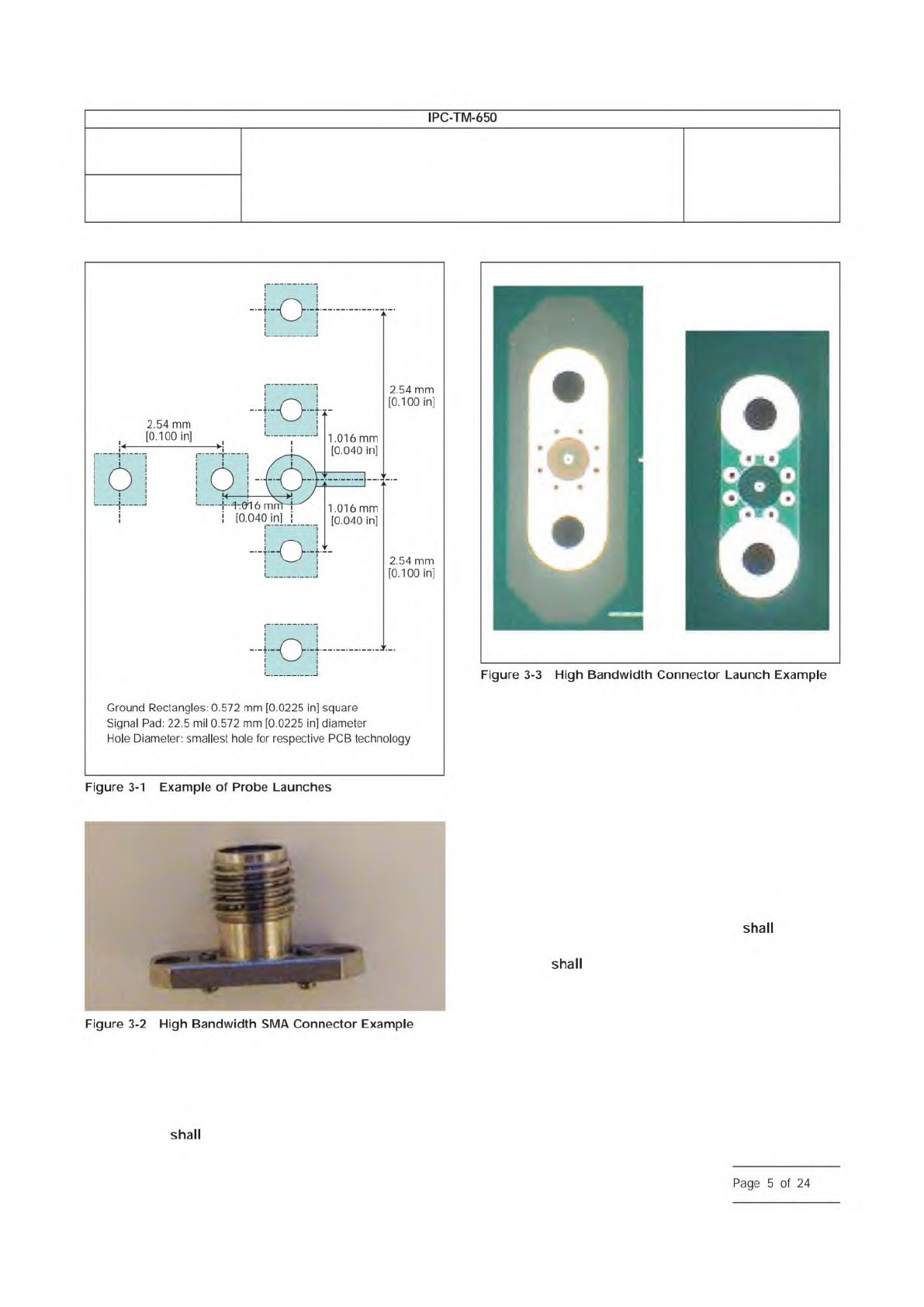
Figure 6 Test Cable Hookup
IPC-TM-650
Number
Subject Date
Revision
Page 3 of 3
2.5.19
Propagation
Delay
of
Flat
Cables
Using
Time
Domain
Reflectometer
7/84
A
IPC-2-5-19-4
—
E
FIR
XPQ
ARE
7
:
E
SECC
XPOE
ND
URE”
i
-
i
l
-Tn
・
j
•一一
1111
1
1
1
1
f
>
f
!
”11
t t
t
t
TDR
STEP
OUT
IN
OUT
I
PC-2-5-1
9-6
divide
the
result
by
10
(distance/time
magnifier
set
at
10)
to
get
the
total
TD
of
the
test
specimen.
Subtract
0.20
ns
x
2
=
0.40
ns
delay
caused
by
the
connection
device
used
at
each
end
of
the
test
cable
and
divide
this
result
by
the
exact
length
of
the
test
specimen
to
get
the
propagation
delay
in
ns/0.3
m.
3.1.7 General Thieving
Thieving which is the use of
nonterminated copper structures, such as planes, pads,
and/or conductors adjacent to test lines that ensure plating
consistency may be used on test coupon. All thieving struc-
tures, if used,
be placed at least six times the width of
the signal conductor (of the test interconnect) or 2.5 mm
[0.100 in], whichever is greater, from each test interconnect.
3.1.8 Termination Types of Test Lines
There are two
types of line styles that may be used. The first is terminated on
each end with a launch. These lines are the only type that are
employed with the SPP and VNA method. The second type of
line is terminated on one end with a launch while the other end
is just the end of a conductor e.g., unterminated. The EBW
and RIE method may use either terminated or unterminated
lines types. The SET2DIL structure requires no termination.
3.1.9 Test Line Routing
The test lines be routed
over/under contiguous ground/voltage planes. The test line
conductors
be kept at least six times the height of the
laminate layer thickness which is closest to the conductor or
2.54 mm [0.100 in], whichever is greater; from printed board
structures include voids, plane splits, other conductors, and
holes.
It is recommended that test lines be straight.
3.1.10 Environmental Conditioning: Temperature and
Humidity
Temperature and humidity effect loss measure-
ments. Consistent results can be obtained by storing test
IPC-25512-3-1
IPC-25512-3-3
Number
2.5.5.12
Subject
Test Methods to Determine the Amount of Signal Loss on
Printed Boards
Date
07/12
Revision
A
IPC-TM-650
—
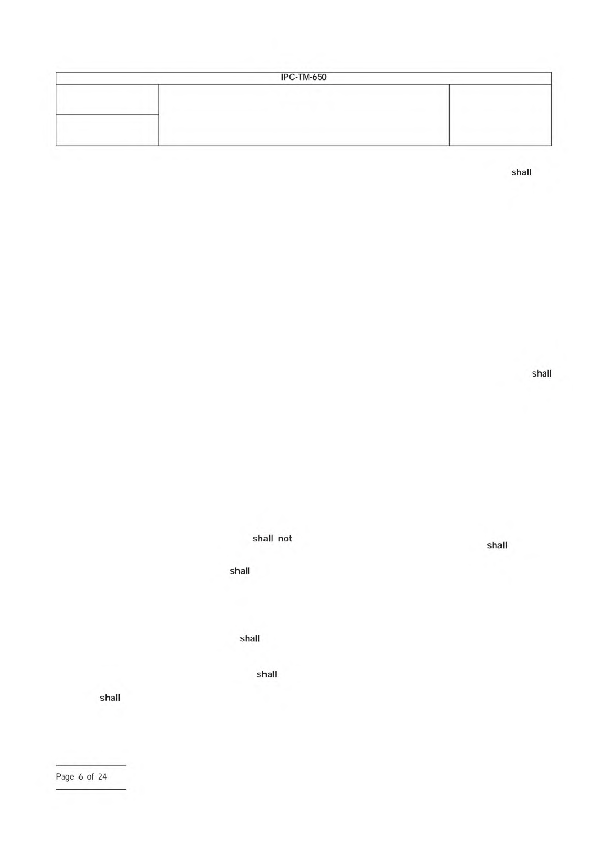
Ground
Rectangles:
0.572
mm
[0.0225
in]
square
Signal
Pad:
22.5
mil
0.572
mm
[0.0225
in]
diameter
Hole
Diameter:
smallest
hole
for
respective
PCB
technology
Figure
3-1
Example
of
Probe
Launches
Figure
3-2
High
Bandwidth
SMA
Connector
Example
Figure
3-3
High
Bandwidth
Connector
Launch
Example
shall
shall
Page
5
of
24
specimens at 23 °C (± 2 °C) [73.4 °F (± 3.6 °F)] and 40% RH
(± 5% RH) for no less than 48 hours.
3.1.11 Fiberweave
It is recommended that the test con-
ductors route at an angle 10 degrees to glass cloth weave.
3.2 Probing
If probing is performed manually, operators
are urged to monitor the oscilloscope trace to ensure proper
connectivity. In the case of SMA connectors that are slip-fit, it
must be ensured that the amplitude of the detected pulse is
unchanged even when a small additional force is applied to
the holding stage movement (within the tolerance of the set-
up) for accurate, repeatable results. In the case of coaxial
probes, a small increase of the z-micropositioner travel (within
the tolerance of the probe allowed force) should also not
change the shape of the pulse. Automated probing can
improve the contact reliability.
For the most part the FD measurements do not use TDR
probes. They employ either connector or microprobes that
have respective calibration kits.
3.3 Test Coupon Characteristics
3.3.1 Test Line Impedance
It is recommended to use
lines that are 50 Ω single ended or 100 Ω differential for SPP.
Using other impedance lines are permitted but the applicabil-
ity is the responsibility or the user. EBW, RIE, SET2DIL, and
FD methods can use other impedances. It is recommended to
limit the line characteristic impedance Z
0
nonuniformity as
measured in TDR to not exceed 20% peak-to-peak along the
length of the lines. The difference in impedance between the
two lines used for SPP and RIE measurement
exceed 5%.
3.3.2 EBW Test Lines
Test lines for EBW be greater
than 5.08 cm [2.00 in] in length. Longer test interconnects
occupy more printed board or panel area. For short intercon-
nects, the relative impact of via loss to other loss effects may
be disproportionably large.
3.3.3 RIE Test Lines
The RIE test sample contain
one transmission (or interconnect) test structure and one ref-
erence transmission line per layer. The Reference is recom-
mended to be 2.54 cm [1.00 in]. The test line
be
between 15.24 cm [6.00 in] and 30.49 cm [12.0 in]. The spe-
cific length
be specified by printed board customers or
vendors. If fold back is required for striplines because of lim-
ited printed board area, maintain maximum spacing of 0.254
cm [0.10 in] between loop back trace legs. Foldbacks are not
recommended for microstrip structures.
3.3.4 SPP Test Structures
SPP test structures have
the following attributes:
• Conductors of varying lengths
• Signal – Ground launch/capture structures
• Disc structures to be used for low frequency capacitance
measurements
3.3.4.1 SPP Test Lines
The goal is to compare the cap-
tured waveforms from two conductors which are as identical
in cross section and laminate building blocks as the manufac-
turing process allows.
The SPP technique relies on the extraction of waveforms from
two different conductor lengths. The specific conductor
lengths used are dependent on the application.
The ratio of the lengths of the long and short conductors
at least be three to one. The following are recommended:
a) 3.0 cm [1.181 in] and 10.0 cm [3.937 in] conductor com-
bination. This combination provides the best output, but it
can be slightly more difficult to find conductors which are
well matched in their physical structure.
b) 2.0 cm [0.787 in] and 8.0 cm [3.149 in] conductor combi-
nation. This combination is useful in thin cards (<0.10 cm
[0.04 in]) for extended high-frequency range when using
coaxial probes for contact.
c) 5.0 cm [1.969 in] and 15.24 cm [6.00 in] conductor com-
bination. This combination is suited for production floor test
coupons.
Printed boards over 0.254 cm [0.1 in] thick
use micro-
vias, back-drilling, top milling or blind vias in order to reduce
the end discontinuities.
3.3.4.2 SSP Disc Structure
A 12.7 mm [0.5 in] diameter
disc is included in the signal layer artwork. The 1 MHz capaci-
tance of this disc is assessed using an LCR meter. The disc
capacitance is assessed through adjacent PTHs, one of which
is attached to the disc by a short conductor; the other is
attached to the reference planes. In the event that both planes
are not at the same reference potential, an isolation border is
placed around the disc structure to prevent shorting two dif-
ferent reference levels.
A ‘‘dummy’’ PTH/conductor structure which is of the same
design as the PTH/conductor used to access the disk is also
included. The capacitance of this dummy structure is sub-
tracted from the capacitance of the disc structure.
Number
2.5.5.12
Subject
Test Methods to Determine the Amount of Signal Loss on
Printed Boards
Date
07/12
Revision
A
IPC-TM-650
shall
not
shall
shall
shall
shall
shall
Page
6
of
24