IPC-TM-650 EN 2022 试验方法--.pdf - 第559页
9) Conduct the short trace characterization from Step 4. 10) Post-p roces s th e r esult s usi ng met hods de scribe d in Section 1 .2.2. Note: The humidity is controlled at RH of 50% (±5%) for all data points, except fo…
Note that an uncertainty estimate of 15% (as an example) is
not meant to suggest that the true insertion loss is within 15%
of the reported value. Rather, the uncertainty estimate is
merely an indicator for the amount of measurement and
de-embedding error evident at any given point.
5.4.5 Determine the Usable Bandwidth of Reported
Insertion Loss
The uncertainty level described in 5.4.4 can
be used to determine the usable bandwidth of the reported
insertion loss. The user can set up an acceptable uncertainty
level based on a specific application, and then examine the
reported insertion loss value at various frequencies, to deter-
mine its usable bandwidth of reported insertion loss (where
the uncertainty level is smaller than the pre-set value).
5.5 Verification of Reported Insertion Loss
Due to
manufacturing variation, and the uncertainties associated with
the calibration/de-embedding process, it is desirable to make
multiple measurements of the same coupon design to
improve the confidence of the measurement results. This is
critical when the material is in a qualification stage and the
amount of manufactured coupons is limited.
One simple approach to verify the reported insertion loss is to
design coupons with multiple lengths on the same board: L1,
L2, and L3. The de-embedding process outlined in 1.2.2 and
1.3 can be applied to any two length combinations:
IL
unit_12
=
|e
-γ (L2–L1)
|
L2–L1
(Eq. 12)
IL
unit_23
=
|e
-γ (L3–L2)
|
L3–L2
(Eq. 13)
IL
unit_13
=
|e
-γ (L3–L1)
|
L3–L1
(Eq. 14)
It is desirable to have the reported insertion loss per unit
length being consistent (e.g., within 5% of each other). A large
discrepancy indicates either problems in measurement/de-
embedding procedures, or a large manufacturing variation
across the board. An average of the above insertion loss num-
ber can be used to report the final value.
It is also important to note that keeping a large length differ-
ence between any two lengths among L1, L2, and L3 will also
help to improve the quality of reported insertion loss.
5.6 Temperature Impact of Insertion Loss
It is known
that the copper conductivity decreases, and the loss tangent
of dielectric material increases with the increase of environ-
mental temperature. Therefore, the insertion loss increases
with the increase of temperature. Meanwhile, the temperature
impact on insertion loss varies with different printed board
materials.
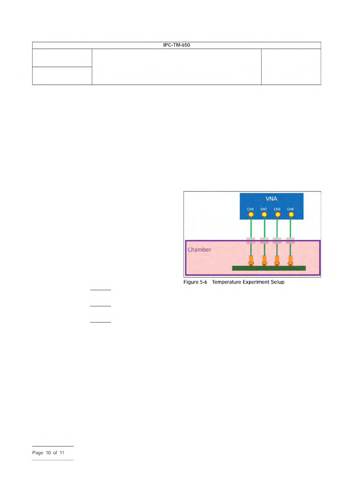
A Test chamber with variable temperature setting is needed.
A suggested temperature range is 0 °C ~ +100 °C, or other-
wise specified by the tester. Temperature accuracy is < ± 1 °C
of actual set point. Humidity accuracy is < ± 5% RH of actual
set point, or otherwise specified by the tester.
It is recommended to use phase-stabilized cables for tem-
perature ranges of 0 °C ~ +100 °C, or otherwise specified by
the tester. Figure 5-6 provides an example of a temperature
experiment setup.
The following procedures describe how to quantify the tem-
perature impact for a given printed board material:
1) Set up VNA equipment according to 5.1.
2) Bake the test coupon at 120 °C over 6 hours.
3) Calibration VNA equipment to the end of cable with
co-axial connector SOLT standards, with the cable
stayed outside the environment chamber.
4) Move cable end through the conduit of chamber and
connect to the long trace of DUT inside the chamber.
Make sure the conduit is sealed with thermal resistant
material after the cable penetrates the chamber. (Note:
high temperature resistant cable should be used)
5) Set the chamber to the target testing temperature and
humidity.
6) Wait at least half an hour to ensure DUT is set to the
ambient temperature
7) Conduct measurement and record data.
8) Moving to the next temperature and humidity setting
(Step 5), until results of all settings are recorded.
IPC-25514-5-6
Number
2.5.5.14
Subject
Measuring High Frequency Signal Loss and Propagation on
Printed Boards with Frequency Domain Methods
Date
02/2021
Revision
IPC-TM-650
Figure
5-6
Temperature
Experiment
Setup
Page
10
of
11

9) Conduct the short trace characterization from Step 4.
10) Post-process the results using methods described in
Section 1.2.2.
Note:
The humidity is controlled at RH of 50% (±5%) for all
data points, except for 0 and 100 °C.
5.7 Test Report
Below is an example of the list of informa-
tion to be included in the test report. The actual format and
information to be included in the test report may vary based
on the requirement of specific customer:
• VNA Settings: test frequency range, step size, IF bandwidth,
etc.
• Probing method: handheld probe, microwave probe, or
printed board mounted co-axial connector without probes
• Manufacturer and part number of the probe (if used), and
the bandwidth of the probe per 4.2
• Condition of test samples per 3.8.1 or 3.8.2
• Temperature and humidity of testing condition for Room-
Temperature test
• Temperature and humidity of testing condition for Varying-
Temperature test per 5.6
• Calibration or de-embedding method per 1.2.2 or 1.3.1 or
1.3.2
• Insertion loss fitting method per 5.4.2 or 5.4.3
• Values of the insertion loss at test frequencies, in dB/inch or
dB/cm
• Uncertainty estimate at test frequencies per 5.4.4
• Any anomalies in the test or variations from this test method
6 Reference Documents
[1] N. R. Franzen, R. A. Speciale, ‘‘A New Procedure for
System Calibration and Error Removal in Automated
S-Parameter Measurements,’’ Proceedings of the 5th
European Microwave Conference, Hamburg, Germany,
1-4 September 1975, pp. 69-73.
[2] R. A. Soares, P. Gouzien, P. Legaud, G. Follot ‘‘A Unified
mathematical approach to two-port calibration tech-
niques and some applications,’’ IEEE Trans. on MTT, v.
37, N 11 1989, pp. 1669-1674.
[3] R. B. Marks, ‘‘A Multiline Method of Network Analyzer
Calibration,‘‘ IEEE Transactions on Microwave Theory
and Techniques 39, pp. 1205-1215, July 1991.
[4] C. Seguinot et al.: – Multimode TRL ‘‘A new concept in
microwave measurements’’
[5] D. Degroot, J. Jargon, R. Marks, ‘‘Multiline TRL
revealed,’’ 60th ARFTG Conference Digest, Fall 2002.
[6] Y. Shlepnev, ‘‘Broadband material model identification
with GMS-parameters’’, 2015 IEEE 24th Conference on
Electrical Performance of Electronic Packaging and Sys-
tems (EPEPS’2015), October 25-28, 2015, San Jose,
CA.
[7] G. F. Engen and C. A. Hoer, ‘‘Thru-Reflect-Line: An
Improved Technique for Calibrating the Dual Six-Port
Automatic Network Analyzer,‘‘ Microwave Theory and
Techniques, IEEE Transactions on, vol. 27, pp.987-993,
1979.
[8] V. Adamian, B. Cole, ‘‘A Novel Procedure for Character-
ization of Multiport High Speed Balanced Devices,’’
DesignCon, San Jose, CA, 2007.
[9] H. Barnes, E. Bogatin, J. Moreira, J. Ellison, et al. ‘‘A
NIST Traceable PCB Kit for Evaluating the Accuracy of
DeEmbedding Algorithms and Corresponding Metrics,’’
DesignCon 2018.
[10] X. Ye, J. Fan and J. Drewniak, ‘‘New De-embedding
Techniques for PCB Transmission-Line Characteriza-
tion’’, DesignCon 2015.
[11] IEEE P370 open-source 2X-Thru de-embedding code,
https://gitlab.com/IEEE-SA/ElecChar/P370.
[12] https://standards.ieee.org/standard/370-2020.html
[13] S. Moon, X. Ye, R. Smith, ‘‘Comparison of TRL Calibra-
tion vs. 2X-Thru De-embedding Methods,’’ IEEE Interna-
tional Symposium on EMC and SI, 2015.
[14] A. Koul, M. Koledintseva, S. Hinaga, J. Drewniak, ‘‘Dif-
ferential Extrapolation Method for Separating Dielectric
and Rough Conductor Losses in Printed Circuit
Boards,’’ IEEE Transaction on Electromagnetic Compat-
ibility, Vol. 54, No. 2, April 2012.
[15] X. Ye, M. Balogh, ‘‘Physics-Based Fitting to Improve
PCB Loss Measurement Accuracy,’’ IEEE International
Symposium on EMC, 2017.
Number
2.5.5.14
Subject
Measuring High Frequency Signal Loss and Propagation on
Printed Boards with Frequency Domain Methods
Date
02/2021
Revision
IPC-TM-650
Page
11
of
11
Number
Subject
Date Revision
Originating Task Group
MaterialinthisTestMethodsManualwasvoluntarilyestablishedbyTechnicalCommitteesofIPC.Thismaterialisadvisoryonly
anditsuseoradaptationisentirelyvoluntary.IPCdisclaimsallliabilityofanykindastotheuse,application,oradaptationofthis
material.Usersarealsowhollyresponsibleforprotectingthemselvesagainstallclaimsorliabilitiesforpatientinfringement.
EquipmentreferencedisfortheconvenienceoftheuseranddoesnotimplyendorsementbyIPC.
3000 Lakeside Drive, Suite 105 N
Bannockburn, Illinois 60015-1249
IPC-TM-650
TEST METHODS MANUAL
1 Scope
This test method describes a way to measure the relative permittivity
(
e
r
) and loss tangent (tan
d
) (also called dielectric constant,
Dk, and dissipation factor, Df) of base materials for printed boards at frequencies from 1 GHz to 20 GHz using a split post
dielectric resonator (SPDR).
2 Applicable Documents
2.1 IPC-TM-650 Method 2.5.5.2 Dielectric Constant and Dissipation Factor of Printed Wiring Board Material –
Clip Method
2.2 IPC-TM-650 Method 2.5.5.3 Permittivity (Dielectric Constant) and Loss Tangent (Dissipation Factor) of Materials
(Two Fluid Cell Method)
2.3 IPC-TM-650 Method 2.5.5.5 Stripline Test for Permittivity and Loss Tangent (Dielectric Constant and Dissipation Factor)
at X-Band
2.4 IPC-TM-650 Method 2.5.5.5.1 Stripline Test for Complex Relative Permittivity of Circuit Board Materials to 14 GHz
2.5 IPC-TM-650 Method 2.5.5.9 Permittivity and Loss Tangent, Parallel Plate, 1MHz to 1.5 GHz
3 Test Specimens
3.1
All base materials specimens shall have the metallic foil layer removed by etching or other suitable means and shall be
thoroughly cleaned. Each specimen shall be marked in the upper left corner with an engraving pencil or equivalent.
3.2
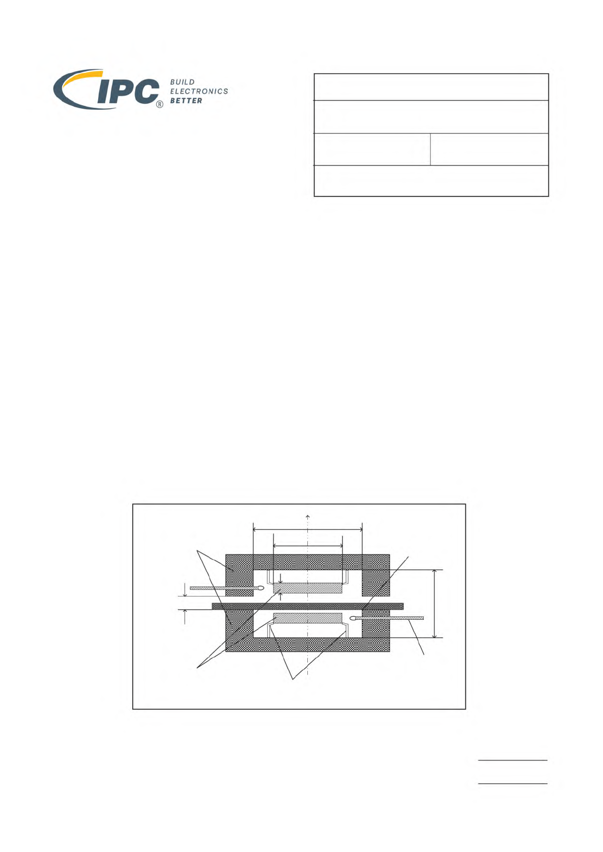
The dimensions of the test specimen shall be larger than the outer dimension of the fixture. See Figure 1.
The size of the specimen shall be larger than the internal diameter D of the metal enclosures, and the maximum thickness of the
specimen shall be smaller than the distance h
g
between the metal enclosures of the fixture.
support
coupling loop
metal enclosure
dielectric resonators
sample
D
h
g
z
h
r
L
dr
Figure1–DiagramofSPDRTestFixture
Page 1 of 7
2.5.5.15
06/22 N/A
3-11aIPC-4101TaskGroup
RelativePermittivityandLossTangentUsinga
Split-PostDielectricResonator
BUILD
ELECTRONICS
BETTER
个