IPC-TM-650 EN 2022 试验方法--.pdf - 第84页
DIN 4768 ISO 4287 Material in this T est M ethods Manual was voluntarily establis hed by T echni cal Committees of IPC. Thi s mat erial is a dvisory only and its use or adaptation is entirely voluntary . IPC disclaims al…
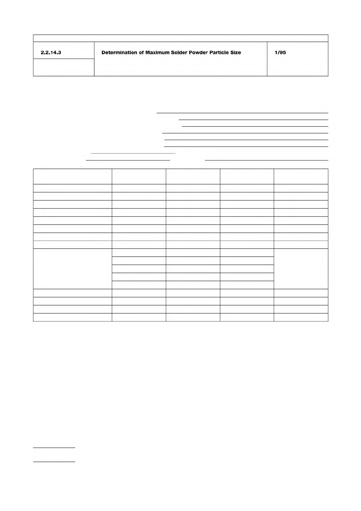
Table 2 Test Report on Solder Paste
Enter appropriate information in top portion of report and complete report by entering the test results or checkmarks in the appropriate spaces.
Inspection Purpose: QPL I.D. Number:
__ Qualification Manufacturer’s Identification:
__ Quality Conformance A Manufacturer’s Batch Number:
__ Quality Conformance B Date of Manufacture:
__ Shelf-Life Extension Original Use-By Date:
__ Performance Revised Use-By Date:
Date Inspection Completed: Overall Results: __ Pass __ Fail
Inspection Performed by:
Witnessed by:
Inspections
User’s Actual
Requirement Test Result P/F (*) Tested by & Date
Material
Visual
Metal Content
Viscosity
Solder Ball
Slump
Alloy
Flux
Powder Size
% In Top Screen
% In Next Screen
% In Bottom Screen
% In Receiver Bottom
Max. Powder Size
Powder Shape
Tack
Wetting
* P/F = PASS/FAIL; enter P if test results are within tolerance of actual requirement; otherwise, enter F
IPC-TM-650
Number
Subject Date
Revision
Page 2 of 2
2.2.14.3
Determination
of
Maximum
Solder
Powder
Particle
Size
1/95
DIN 4768
ISO 4287
Material in this Test Methods Manual was voluntarily established by Technical Committees of IPC. This material is advisory only
and its use or adaptation is entirely voluntary. IPC disclaims all liability of any kind as to the use, application, or adaptation of this
material. Users are also wholly responsible for protecting themselves against all claims or liabilities for patent infringement.
Equipment referenced is for the convenience of the user and does not imply endorsement by IPC.
Page 1 of 2
r
ASSOCIATION
CONNECTING
/
ELECTRONICS
INDUSTRIES
221
5
Sanders
Road
Northbrook,
IL
60062-6135
IPC-TM-650
TEST
METHODS
MANUAL
1
Scope
This
method
defines
the
procedure
for
determin¬
ing
the
roughness
or
profile
of
metallic
foils.
1.1
The
surface
finish
or
roughness
of
foils
shall
be
evalu¬
ated
using
Ra.
Ra
is
defined
as
the
arithmetic
average
value
of
all
absolute
distances
of
the
roughness
profile
from
the
center
line
within
the
measuring
length.
1.2
The
foil
profile
of
foils
shall
be
evaluated
using
the
parameter
Rz
(DIN)
or
RTM,
which
is
defined
as
the
average
maximum
peak
to
valley
height
of
five
consecutive
sampling
lengths
within
the
measurement
length.
This
value
is
approxi¬
mately
equivalent
to
the
values
of
profile
determined
from
microsectioning
techniques.
1.3
Rz
(ISO)
is
a
different
parameter
from
Rz
(DIN)
and
is
not
applicable
to
this
method.
2
Applicable
Documents
3
Test
Specimens
Cut
a
specimen
101
x
101
mm
[4x4
in]
minimum
from
the
representative
sample.
The
location
and
number
of
specimens
shall
be
defined
in
the
material
specifi¬
cation.
4
Apparatus/Materials
4.1
Knife
or
other
suitable
device.
4.2
Profilometer
or
surface
roughness
meter
with
a
motor¬
ized
drive
and
the
following
parameters:
Parameter
Gut
Off
Measuring
Length
Tracing
Length
Diamond
Stylus
Radius
Value
0.8
mm
4.0
mm
<5
mm
0.005
mm
Number
2.2.1
7A
Subject
Surface
Roughness
and
Profile
of
Metallic
Foils
(Contacting
Stylus
Technique)
Date
Revision
2/2001
A
Originating
Task
Group
Metallic
Foils
Task
Group
(3-1
2
A)
Roughness
Parameter
Ra,
per
1.1
R/din
or
Rtm,
per
1
Note:
See
Footnote
No.
1
for
equipment
found
suitable
for
determination
of
both
Ra
and
RZD,N
(or
RTM).3
1
4.3
Roughness
Standard
Smooth
Side:
Ra
with
5%
or
better
certified
tolerance
Treated
Side:
Rdzin
(or
Rtm)
with
5%
or
better
certified
toler¬
ance
4.4
Plate
glass
or
other
smooth
flat
surface
4.5
Compressed
air
4.6
Gloves,
lint
free
4.7
Tape
or
weight
5
Procedure
5・1
Check
the
profilometer
calibration
using
the
appropriate
roughness
standard
for
the
value
Ra
or
RZD,N
(RTM)
and
mag¬
nitude
to
be
measured.
Insure
the
stylus
moves
perpendicular
to
the
grooves
and
the
surface.
Note:
For
Rz
measurements,
known
standards
are
available
in
1
,
3
and
1
0
micrometer
nominal
values.
See
footnote
2.2
5.1.1
Compare
the
values
obtained
on
six
different
mea¬
surements
taken
at
different
locations
within
the
standard
to
the
certified
(not
nominal
value)
of
the
standard.
If
the
average
result
is
not
within
2%
of
the
standard
value,
adjust
the
instru¬
ment
and
repeat
5.1
until
this
tolerance
is
achieved.
5.2
Place
the
foil
test
specimen
on
the
plate
glass
surface
with
the
side
to
be
tested
away
from
the
glass.
Secure
the
specimen
with
tape
or
a
weight
at
both
ends
to
prevent
move¬
ment
or
buckling
during
the
measurement.
1
.
Profilometers
which
have
been
used
to
measure
both
Ra
and
Rz
or
RTM
are:
Surtronic
3
by
Taylor
Hobson
(Ra
and
RTM)
(see
8.2);
M4P
by
Perthen
(see
8.1)
(Ra
and
Rzdin)-
2.
Standards
for
RDZ)N
are
available
from:
see
8.1
,
PGN-3
3
micrometer
nominal,
PGN-10
10
micrometer
nominal.
IPC-TC-500
NOTE:
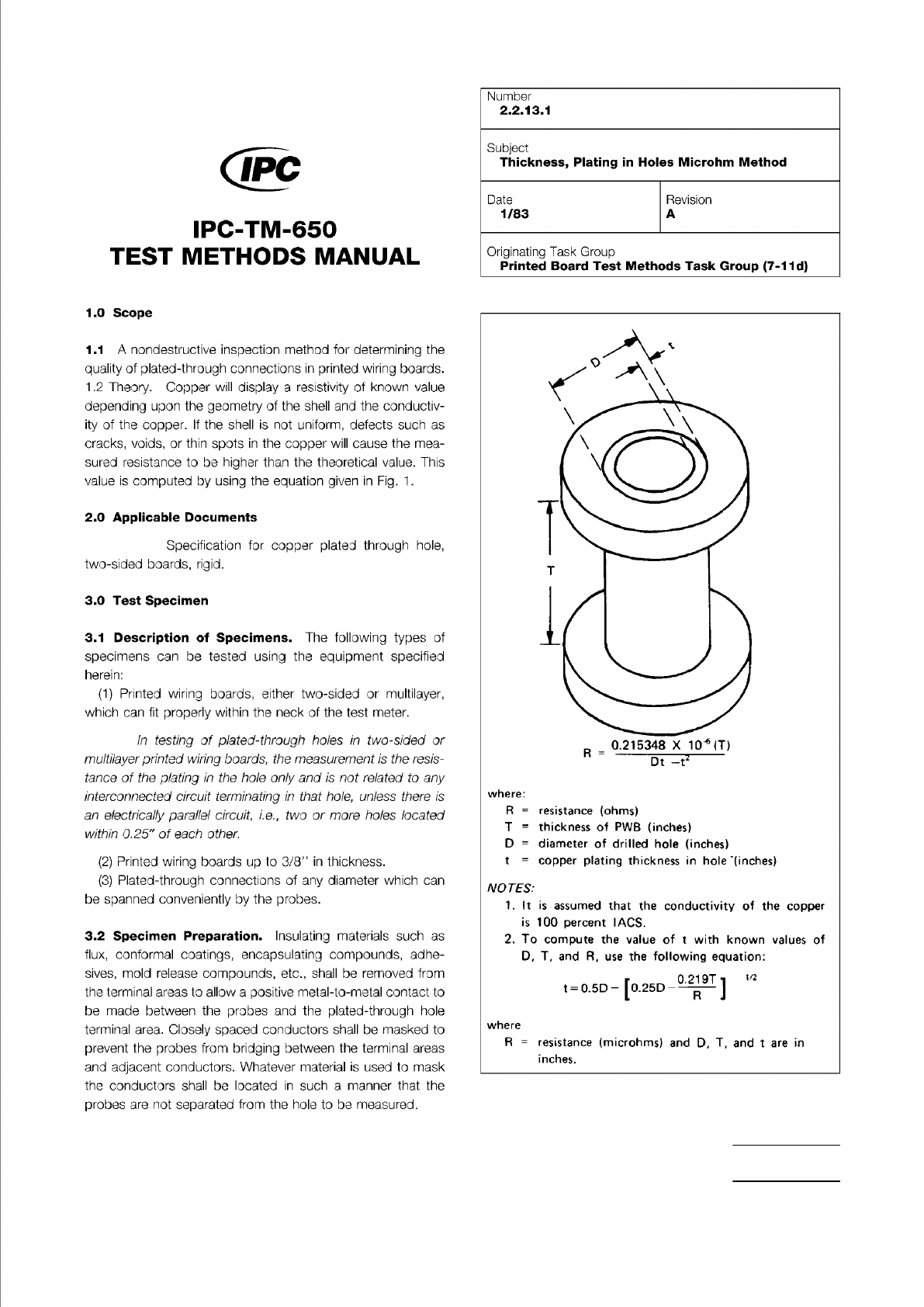
Figure 1 Resistance Calculation of Plated-Through
Connection
The Institute for Interconnecting and Packaging Electronic Circuits
2215 Sanders Road • Northbrook, IL 60062
Material in this Test Methods Manual was voluntarily established by Technical Committees of the IPC. This material is advisory only
and its use or adaptation is entirely voluntary. IPC disclaims all liability of any kind as to the use, application, or adaptation of this
material. Users are also wholly responsible for protecting themselves against all claims or liabilities for patent infringement.
Equipment referenced is for the convenience of the user and does not imply endorsement by the IPC.
Page 1 of 4
IPC-TM-650
TEST
METHODS
MANUAL
1
.0
Scope
1.1
A
nondestructive
inspection
method
for
determining
the
quality
of
plated-through
connections
in
printed
wiring
boards.
1
.2
Theory.
Copper
will
display
a
resistivity
of
known
value
depending
upon
the
geometry
of
the
shell
and
the
conductiv¬
ity
of
the
copper.
If
the
shell
is
not
uniform,
defects
such
as
cracks,
voids,
or
thin
spots
in
the
copper
will
cause
the
mea¬
sured
resistance
to
be
higher
than
the
theoretical
value.
This
value
is
computed
by
using
the
equation
given
in
Fig.
1
.
2
.0
Applicable
Documents
Specification
for
copper
plated
through
hole,
two-sided
boards,
rigid.
3
.0
Test
Specimen
3.1
Description
of
Specimens.
The
following
types
of
specimens
can
be
tested
using
the
equipment
specified
herein:
(1)
Printed
wiring
boards,
either
two-sided
or
multilayer,
which
can
fit
properly
within
the
neck
of
the
test
meter.
In
testing
of
plated-through
holes
in
two-sided
。广
multilayer
printed
wiring
boards,
the
measurement
is
the
resis¬
tance
of
the
plating
in
the
hole
only
and
/s
not
related
to
any
interconnected
circuit
terminating
in
that
hole,
unless
there
is
electrically
parallel
circuit,
ie,
two
or
more
holes
located
within
0.25"
of
each
other.
(2)
Printed
wiring
boards
up
to
3/8"
in
thickness.
(3)
Plated-through
connections
of
any
diameter
which
can
be
spanned
conveniently
by
the
probes.
3.2
Specimen
Preparation.
Insulating
materials
such
as
flux,
conformal
coatings,
encapsulating
compounds,
adhe¬
sives,
mold
release
compounds,
etc.,
shall
be
removed
from
the
terminal
areas
to
allow
a
positive
metal-to-metal
contact
to
be
made
between
the
probes
and
the
plated-through
hole
terminal
area.
Closely
spaced
conductors
shall
be
masked
to
prevent
the
probes
from
bridging
between
the
terminal
areas
and
adjacent
conductors.
Whatever
material
is
used
to
mask
the
conductors
shall
be
located
in
such
a
manner
that
the
probes
are
not
separated
from
the
hole
to
be
measured.
Number
2.2.13.1
Subject
Thickness,
Plating
in
Holes
Microhm
Method
Date
1/83
Revision
A
Originating
Task
Group
Printed
Board
Test
Methods
Task
Group
(7-1
Id)
where:
R
=
resistance
(ohms)
T
=
thickness
of
PWB
(inches)
D
=
diameter
of
drilled
hole
(inches)
t
=
copper
plating
thickness
in
hole
'(inches)
NOTES:
1.
It
is
assumed
that
the
conductivity
of
the
copper
is
100
percent
I
ACS.
2.
To
compute
the
value
of
t
with
known
values
of
D,
T,
and
R,
use
the
following
equation:
t
=
0.5D-[0.25D-^I]
-
where
R
=
resistance
(microhms)
and
D,
T,
and
t
are
in
inches.