IPC-TM-650 EN 2022 试验方法--.pdf - 第675页
IPC-TM-650 Page 3 of 4 Number 2.6.3.5 Subject Bare Board Cleanliness by Surface Insulation Resistance Date 01/04 Revision After 96 hours total, repeat the measurement series. Regard¬ less of the outcome of the measuremen…
NOTE:
NOTE:
Figure 3 IPC-B-50
IPC-TM-650
Page 2 of 4
Number
2.6.3.5
Subject
Bare
Board
Cleanliness
by
Surface
Insulation
Resistance
Date
01/04
Revision
4.2
A
resistance
meter
capable
of
reading
high
resistance
(1012ohms)
with
a
test
voltage
of
100
±
2
volts
DC
or
an
ammeter
capable
of
reading
10-10
amperes
in
combination
with
1
00
volts
DC
power
supply.
Standard
resistors
should
be
used
for
routine
calibration.
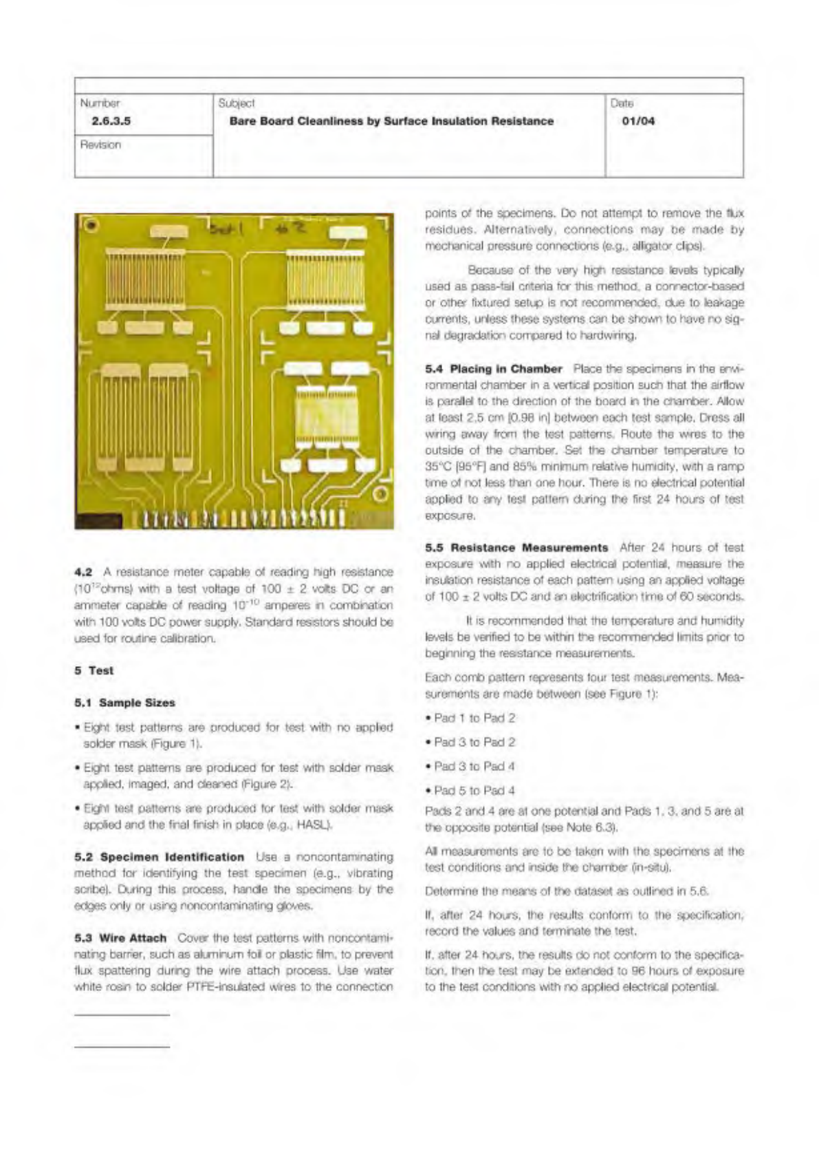
5
Test
5.1
Sample
Sizes
•
Eight
test
patterns
are
produced
for
test
with
no
applied
solder
mask
(Figure
1).
•
Eight
test
patterns
are
produced
for
test
with
solder
mask
applied,
imaged,
and
cleaned
(Figure
2).
•
Eight
test
patterns
are
produced
for
test
with
solder
mask
applied
and
the
final
finish
in
place
(e.g.,
HASL).
5.2
Specimen
Identification
Use
a
noncontaminating
method
for
identifying
the
test
specimen
(e.g.,
vibrating
scribe).
During
this
process,
handle
the
specimens
by
the
edges
only
or
using
noncontaminating
gloves.
5.3
Wire
Attach
Cover
the
test
patterns
with
noncontami¬
nating
barrier,
such
as
aluminum
foil
or
plastic
film,
to
prevent
flux
spattering
during
the
wire
attach
process.
Use
water
white
rosin
to
solder
PTFE-insulated
wires
to
the
connection
points
of
the
specimens.
Do
not
attempt
to
remove
the
flux
residues.
Alternatively,
connections
may
be
made
by
mechanical
pressure
connections
(e.g.,
alligator
clips).
Because
of
the
very
high
resistance
levels
typically
used
as
pass-fail
criteria
for
this
method,
a
connector-based
or
other
fixtured
setup
is
not
recommended,
due
to
leakage
currents,
unless
these
systems
can
be
shown
to
have
no
sig¬
nal
degradation
compared
to
hardwiring.
5.4
Placing
in
Chamber
Place
the
specimens
in
the
envi¬
ronmental
chamber
in
a
vertical
position
such
that
the
airflow
is
parallel
to
the
direction
of
the
board
in
the
chamber.
Allow
at
least
2.5
cm
[0.98
in]
between
each
test
sample.
Dress
all
wiring
away
from
the
test
patterns.
Route
the
wires
to
the
outside
of
the
chamber.
Set
the
chamber
temperature
to
35℃
[95°F]
and
85%
minimum
relative
humidity,
with
a
ramp
time
of
not
less
than
one
hour.
There
is
no
electrical
potential
applied
to
any
test
pattern
during
the
first
24
hours
of
test
exposure.
5.5
Resistance
Measurements
After
24
hours
of
test
exposure
with
no
applied
electrical
potential,
measure
the
insulation
resistance
of
each
pattern
using
an
applied
voltage
of
1
00
±
2
volts
DC
and
an
electrification
time
of
60
seconds.
It
is
recommended
that
the
temperature
and
humidity
levels
be
verified
to
be
within
the
recommended
limits
prior
to
beginning
the
resistance
measurements.
Each
comb
pattern
represents
four
test
measurements.
Mea¬
surements
are
made
between
(see
Figure
1):
•
Pad
1
to
Pad
2
•
Pad
3
to
Pad
2
•
Pad
3
to
Pad
4
•
Pad
5
to
Pad
4
Pads
2
and
4
are
at
one
potential
and
Pads
1
,
3,
and
5
are
at
the
opposite
potential
(see
Note
6.3).
All
measurements
are
to
be
taken
with
the
specimens
at
the
test
conditions
and
inside
the
chamber
(in-situ).
Determine
the
means
of
the
dataset
as
outlined
in
5.6.
If,
after
24
hours,
the
results
conform
to
the
specification,
record
the
values
and
terminate
the
test.
If,
after
24
hours,
the
results
do
not
conform
to
the
specifica¬
tion,
then
the
test
may
be
extended
to
96
hours
of
exposure
to
the
test
conditions
with
no
applied
electrical
potential.
IPC-TM-650
Page 3 of 4
Number
2.6.3.5
Subject
Bare
Board
Cleanliness
by
Surface
Insulation
Resistance
Date
01/04
Revision
After
96
hours
total,
repeat
the
measurement
series.
Regard¬
less
of
the
outcome
of
the
measurements,
the
test
terminates
after
this
measurement
series.
5.6
Data
Analysis
The
average
insulation
resistance
(IRavg)
is
calculated
as
follows:
IRavg
=
1
°
•
N
•
N
£iogio(iR>
1
Where:
N
=
Number
of
Test
Points
(32
nominal
for
each
set
of
eight
patterns)
IRi
=
individual
insulation
resistance
measurements
See
6.4
for
an
example
No
individual
insulation
resistance
value
may
be
more
than
a
factor
of
1
0
below
the
specified
minimum
value.
Where
an
assignable
cause
of
low
insulation
resistance,
which
is
properly
attributable
to
the
laminate
itself,
or
to
the
process
used
to
produce
the
PWB,
can
be
found,
then
such
a
value
can
be
excluded
from
calculating
the
average
value,
provided
that
at
least
30
test
points
are
included
in
the
average.
Such
assignable
causes
include
the
following:
•
Contamination
on
the
insulating
surface
of
the
board,
such
as
lint,
solder
splines
or
water
droplets
from
the
chamber.
•
Incompletely
etched
patterns
that
decrease
the
insulating
space
between
the
conductors
by
more
than
the
amount
allowed
in
the
appropriate
design
requirements
drawing.
•
Scratched,
cracked,
or
obviously
damaged
insulation
between
conductors.
6
Notes
6.1
If
condensation
occurs
on
the
test
specimens
in
the
environmental
chamber
while
the
samples
are
under
voltage,
dendritic
growth
will
occur.
This
can
be
caused
by
a
lack
of
sufficient
control
of
the
humidification
of
the
oven.
Water
spot¬
ting
may
also
be
observed
in
some
ovens
where
the
airflow
in
the
chamber
is
from
back
to
front.
In
this
case,
water
conden¬
sation
on
the
cooler
oven
window
can
be
blown
around
the
oven
as
microdroplets
which
deposit
on
test
specimens
and
cause
dendritic
growth
if
the
spots
bridge
the
distance
between
two
electrified
conductors.
Both
of
these
conditions
must
be
eliminated
for
proper
testing.
6.2
Tight
control
of
the
test
humidity
is
critical
for
this
test
method.
A
difference
of
5%
relative
humidity
can
result
in
a
0.5
-
1
.0
decade
difference
in
the
measured
resistance.
The
uniformity
of
the
environment
is
also
important.
A
fully
loaded
chamber,
where
airflow
is
severely
impeded,
may
have
a
30-40%
RH
range
within
the
chamber
workspace.
6.3
The
polarity
of
the
applied
voltage
is
not
important
as
long
as
the
application
is
consistent
(e.g.,
Pads
1,
3,
5
are
positive
and
2,
4
are
at
opposite
potential,
vs.
Pads
2
and
4
positive,
and
Pads
1
,
3,
5
at
opposite
potential).
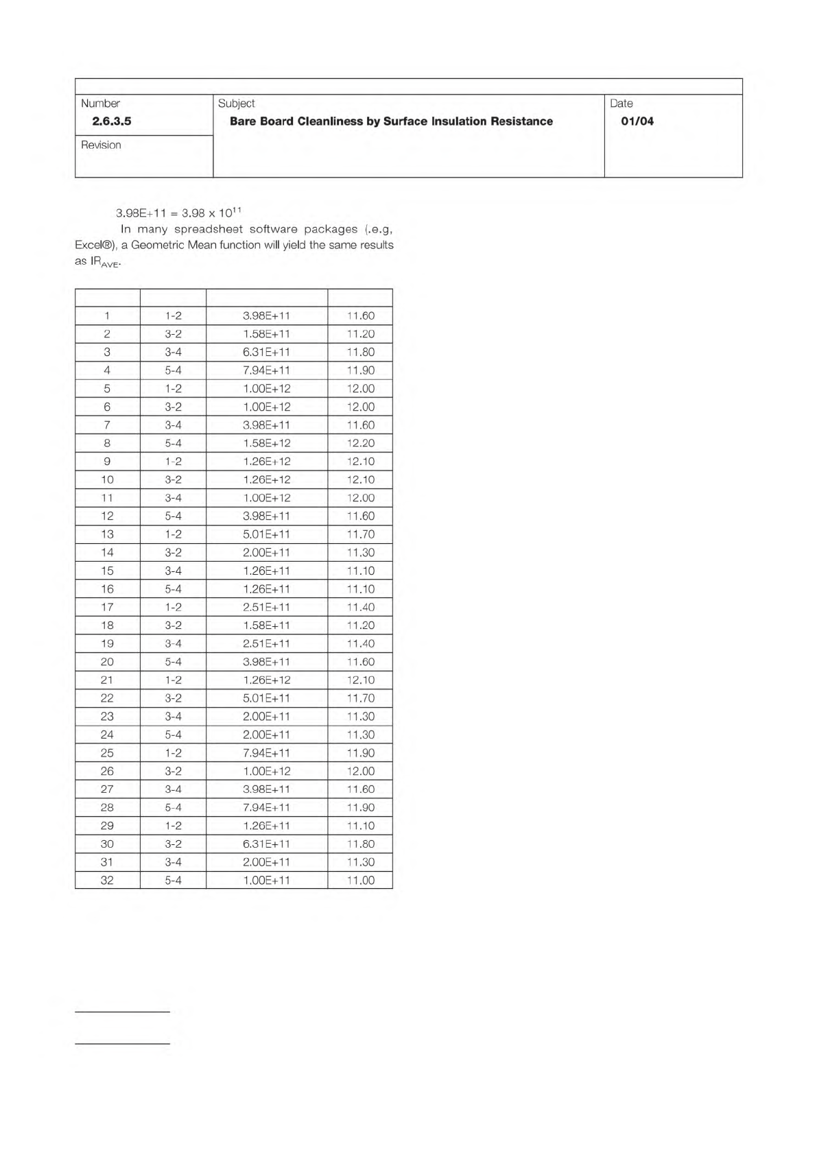
6.4
Example
of
Numerical
Calculations
Eight
5-point
test
patterns
(4
measurements
each)
LogOhms
二
base-
10
logarithm
of
measured
resistance
Average
of
LogOhms
=
11
.62
IRave
二
Antilog
(1
1
.62)
=
4.19E+1
1
ohms
IRave
二
Geometric
Mean
NOTE:
NOTE:
No. Pattern Resistance (Ohms) LogOhms
IPC-TM-650
Page 4 of 4
Number
2.6.3.5
Subject
Bare
Board
Cleanliness
by
Surface
Insulation
Resistance
Date
01/04
Revision
3.98E+11
=
3.98
x
1011
In
many
spreadsheet
software
packages
(.e.g,
Excel®),
a
Geometric
Mean
function
will
yield
the
same
results
1
1-2
3.98E+11
11.60
2
3-2
1
.58E+1
1
11.20
3
3-4
6.31
E+11
11.80
4
5-4
7.94E+11
11.90
5
1-2
1.00E+12
12.00
6
3-2
1.00E+12
12.00
7
3-4
3.98E+11
11.60
8
5-4
1.58E+12
12.20
9
1-2
1.26E+12
12.10
10
3-2
1.26E+12
12.10
11
3-4
1.00E+12
12.00
12
5-4
3.98E+1
1
11.60
13
1-2
5.01
E+11
11.70
14
3-2
2.00E+11
11.30
15
3-4
1.26E+11
11.10
16
5-4
1.26E+11
11.10
17
1-2
2.51
E+11
11.40
18
3-2
1
.58E+1
1
11.20
19
3-4
2.51
E+11
11.40
20
5-4
3.98E+1
1
11.60
21
1-2
1.26E+12
12.10
22
3-2
5.01
E+11
11.70
23
3-4
2.00E+1
1
11.30
24
5-4
2.00E+11
11.30
25
1-2
7.94E+11
11.90
26
3-2
1.00E+12
12.00
27
3-4
3.98E+11
11.60
28
5-4
7.94E+11
11.90
29
1-2
1.26E+11
11.10
30
3-2
6.31
E+11
11.80
31
3-4
2.00E+11
11.30
32
5-4
1
.00E+1
1
11.00