创建组件识别数据的方法.pdf - 第122页
122/178 IM-SMT-VSNDI C-0002 -000 and the center of the com ponent is larger than the Min. Bri ghtness Diff erence (brightness of the outer peri phery – brightness of the c enter > Min. Bri ghtness Difference), the res…
121/178
IM-SMT-VSNDIC-0002-000
The detection circle used to differentiate the direction is set as the first Lead
Group in the East direction if the leads are placed vertically, and in the North
direction if they are placed horizontally.
- Number of Lead Group: 1
- Number of leads: 0
- Lead length: 0
- Lead width: Diameter of detection circle (mm)
- Lead pitch: 0
- Lead reference position X: Detection circle center position X
- Lead reference position Y: Detection circle center position Y
Based on the results obtained from the “Direction check”, add +90°, +180° or +270° to
the tilt of the component and set the value to the fields of “Lead Width” and “Lead
reference position X, Y”.
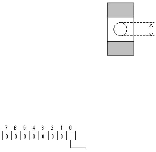
(4) Special 4: Nozzle check (check the center of the chip)
Option 2: Threshold used for check (0 ~ 255)
Option 3: Diameter of the detected region
1 - 255 (unit: 0.1 mm -> allowable setting range: 0.1 mm - 25.5. mm)
Option 4: NG Condition (0: Less than threshold, 1: More than threshold)
Figure 96
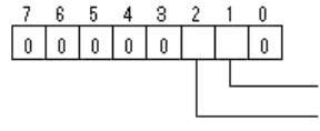
(5) Special 5: Retry Lead Center Search
When detecting the edge in the lead width direction, the recognition is performed several
times while changing the detection line position slightly each time, and the value closest to
the component data is adopted as the result.
Option 1: Recognition Flag
(6) Special 6: Check Upside-Down
This checks the difference between the brightness of the outer periphery of the component
and the center of the component in order to identify the top surface and bottom surface of the
component.
Option 1: Min. Brightness Difference
If the difference between the brightness of the outer periphery of the component
Bit position
Angle Correction: (0:None, 1: Exist)
122/178
IM-SMT-VSNDIC-0002-000
and the center of the component is larger than the Min. Brightness Difference
(brightness of the outer periphery – brightness of the center > Min. Brightness
Difference), the result is satisfactory.
Option 2: Brightness threshold of center area
If the brightness of the component center is smaller than the Brightness
threshold of center area, the result is satisfactory. (0 is not checked)
(7) Special 7: Not supported
(8) Special 8: Chip Array
Option 1: (0: Convex electrode type, 1: Concave electrode type (Not supported),
2: Flat electrode type (C array))
(9) Special 9: Not supported
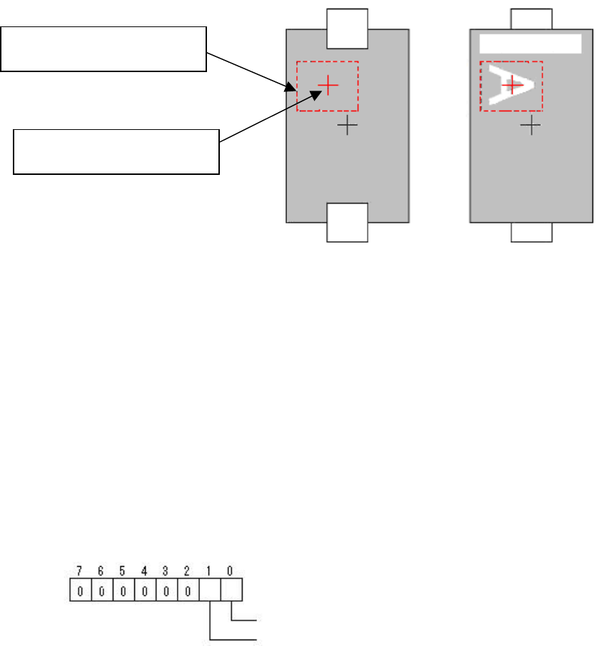
(10) Special 10: Check Upside-Down of Diode
This checks the variation of the brightness (dispersion) of the determination area in order
to identify the top surface and the bottom surface of the component.
It is applicable for the components with the characters printed on the molded area of the
pickup surface such as 2-terminal diodes.
Option 1: Threshold of 3-sigma
This sets the threshold of the brightness variance (3 sigma) in the determination
area. The variance becomes larger as the variation of the brightness becomes
larger.
Option 2: Threshold of Average
This sets the lower limit of the average threshold (Ave) of the determination area.
It is available only when “Dispersion” is selected from the “NG condition” item,
and is used to avoid the over-determination when judged by the variance.
Option 3: Judgment Flag
(Some old versions of software may not be equipped with this function.)
Dispersion: When the brightness variance is larger than the threshold in the
determination area, it is determined to be an error.
Non Dispersion: When the brightness variance is smaller than the threshold in the
determination area, it is determined to be an error.
The determination area is set to the “Lead Group 1” in the W direction.
(When it is required to offset to the East direction, set to E direction.)
- Number of the Lead Group W: 1
- Number of the leads W1: 0
- Lead Pitch W1: 0
- Lead Width W1: Determination area size Y
- Reflct LL W1: Determination area size X
- Find Pos X W1: Check Area Offset X
- Find Pos Y W1: Check Area Offset Y
Bit position
Check
-
Area Offset Enable:(0: Disable, 1: Enable)
NG condition: (0: Dispersion, 1: Non Dispersion)
123/178
IM-SMT-VSNDIC-0002-000
Figure 97
Special 11: Not supported
Special 12: Size Fitting (Bare chip )recognition
This is used for recognition of chip components. It detects the object whose size is
close to the defined component size by changing the threshold. It can also be used for
direction discrimination.
<Example of the setting for direction discrimination>
- Lead Group N: 2
- Number of the leads N2: Number of the brightness measurement area (circle)
- Lead Pitch N2: Pitch of the measurement area
- Lead Width N2: The diameter of the brightness measurement area (circle)
- Find Pos X: The coordinate of start point X in the brightness measurement area
- Find Pos Y: The coordinate of start point Y in the brightness measurement area
Option 1: Setting Flag
Option 2: The “Min. Brightness Difference” in the brightness measurement area
(When the value “0” is specified, the value “50” is adopted as default.)
Special 13: Not supported
Special 14: Not supported
Special 15: Check Many Adsorption
This detects whether more than one component is picked up by checking around
the detected chip component. The thickness of the actual component needs to be
input accurately as the distance to be checked varies depends on the component
thickness.
Determination area size Y
Determination area size X
Check Area Offset X
Check Area Offset Y
Bit position
Check Type: (0:Black, 1: White)
Check Direction: (0:
(0°, 180°), 1: (0°, 90°, 180°, 270°)
Picked up
properly
Not properly
picked up