OptimaUserManual.pdf - 第121页
OPT IMA PAL SO FTW ARE Opti ma User M anual 115 veri fication) of the devi ce. This means that the patter n set into the fuses of the device is no long er readable by personnel who are not authorized to vi ew the data pa…
OPTIMA PAL SOFTWARE
Optima User Manual
114
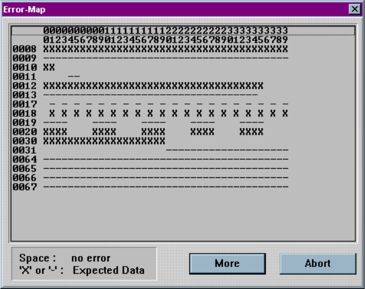
If you select <YES>, then the following screen appears:
Device error map following a verify failure
On the screen above, there are indications of the device locations and the failures
encountered. Blank spaces indicate locations where the data matched. Any space
with either a “–” symbol or an “X” symbol is an error, where the symbols indicate the
data that was expected in that location (“–” = blown fuse, “X” = connected fuse). The
<More> button provides more failure data if it exceeds the capacity of the window. If
a device has been secured, the Verify operation will not function correctly.
Device>Secure
This selection manually sets the security feature of the device inserted in the socket.
Many logic devices have optional security fuses that can be programmed after all
other fuses have been programmed. These final fuses prohibit reading (and
OPTIMA PAL SOFTWARE
Optima User Manual
115
verification) of the device. This means that the pattern set into the fuses of the device
is no longer readable by personnel who are not authorized to view the data pattern.
To manually secure the device, select Device>Secure. This must be the last step in
any programming sequence since the programmer expects to able to verify (read) a
device after programming.
In automatic mode (set with the Auto Security selection in the Options menu), the
security fuse(s) will be set during each programming cycle, after verifying and before
vector testing. If the JEDEC file contains the security fuse command (G1*), the Auto
Security mode is automatically enabled, and the Auto Security feature will be
checked in the Options menu.
The PAL software first programs the security fuse, then reads the array to verify that
the data no longer matches the array. The PASS message will only be displayed if the
array data is no longer readable.
Some devices disable preload if the security fuse is set. For these devices, Optima
PAL will run the test vector program before setting the security fuse during the
programming routine.
Some devices have a mode to read out the security fuse bit. Optima PAL can read this
bit and will indicate that the security bit is set. However, it will then perform a
double-check of the array contents to assure protection.
Device>Test
This selection performs vector testing of the device after programming. If a JEDEC
file with test vectors has been read into memory, then the device in the socket can be
tested for conformance with these test sequences with this command. This test will
also be invoked after the Verify operation in a programming cycle if test vectors are in
memory.
Note: If no test vectors are appended to the JEDEC file, this option
is not enabled.
The Test operation has three passes for each vector. Pass 1 sets up all input pins.
Any 0, 1, or X levels are presented to the device. All device outputs are set to read
mode. Optima PAL has a special method for handling the “X” (don’t care) level,
which is incompletely defined in the JEDEC specification and is often a cause of
vector test failures in other systems.
OPTIMA PAL SOFTWARE
Optima User Manual
116
Pass 2 applies any clocks to the device. The vector is scanned from highest pin to
lowest pin, and the clocks are output in that order. If a multiple click device requires a
controlled sequence of clocks, then there should be a separate vector for each clock.
It is impossible for a universal programmer like the Optima programmer to generate
simultaneous clocks on two pins. There will always be a time spacing between
multiple clocks in a test vector. Note that the “C” clock is normally low, and the “K”
clock is normally high.
Pass 2 also executes the preload function if a P or B vector is found. A P or B in pin1
of the vector indicates preload. Note that entering and leaving preload mode can
generate transient logic levels that can have other effects in a PAL design.
Pass 3 verifies the outputs of the devices against the test vector. If there are no errors,
the next vector is processed. If there are any errors, the good and bad data will be
displayed on the screen, and testing will stop unless continued by you.
Pins defined as “X” in the vectors are set as inputs to “0” unless the pin is determined
to be an unused output, in which case it is floated. High impedance outputs are tested
for incorrect “0” conditions, but not for low impedance “1” conditions. Test
simulation can also be used to verify a device after the security fuse has been
programmed (note that AMD PALCE-family of devices disables preload when
security is set).