YesAX V3.1.2 - Software User Manual.pdf - 第117页
General Inspecti on Methodolo gy 10 - 23 Update Uses the current solder box as reference to update other solder boxes on other parts. To Inspect Position During review mode, this option will reset the camera position to …
10-22 General Inspection Methodology
The Solder Thickness Compensation Calculation is for solder thickness compensation
purpose. It won’t be enabled if the following two fields: No Solder Gray Level and High
Pitch/Roll Threshold are filled with 0 or the solder inspection box has a width less than Comp.
Area Min Width (250 in pixels) or a height less than Min Height (200 in pixels). In reality the
solder thickness of a solder joint is not even. For example, if the component is tilted in one way,
then along that direction the thickness of the solder area will gradually increase or decrease,
which causes the unevenness of the image. If a void is located at relatively thick solder area, it
may even appears darker than some thin solder areas without any void at all. This will make void
detection more difficult. The solder thickness calculation is designed to compensate for the
unevenness of the solder layer.
To make it work, first the user needs to set up the No Solder Gray Level, which represents the
average gray levels for areas without any solder. To set up Thickness Per Gray Level, some
calculation needs to be done first. If the thickness of solder is 500µm (this number can be
acquired by doing laser height measurement on solder area), and the gray levels for such amount
of solder is 50, then the Thickness Per Gray Level will be 10µm/Gray (500/50). Once the pitch
and roll have been calculated, the results will be compared with High Pitch/Roll Threshold
first. Only numbers bigger than the preset threshold value will be used for thickness
compensation. If the numbers are smaller, it is reasonable to assume that the numbers are not
reliable thus the user will choose rather not doing the compensation at all. The results of Pitch
and Roll can be seen on the percent void result dialog, together with the inspection results.
Sometime there is certain area inside the ROI that the user does not want to inspect. To mask out
the area the user can enable the Use Mask option, select either Ellipse or Rectangle as shape
indicator and then click Set button to define the mask area. The mask area does not need to be
totally reside inside the ROI and the mask out area will be subtracted from the total area
calculate.
Solder Alignment.
Move/Resize
Moves and/or Resizes the solder inspection box.
Delete
Deletes the current solder.
General Inspection Methodology 10-23
Update
Uses the current solder box as reference to update other solder boxes on other parts.
To Inspect
Position
During review mode, this option will reset the camera position to the original position the
inspection box was tested in.
Test
Inspects the solder on the current image.
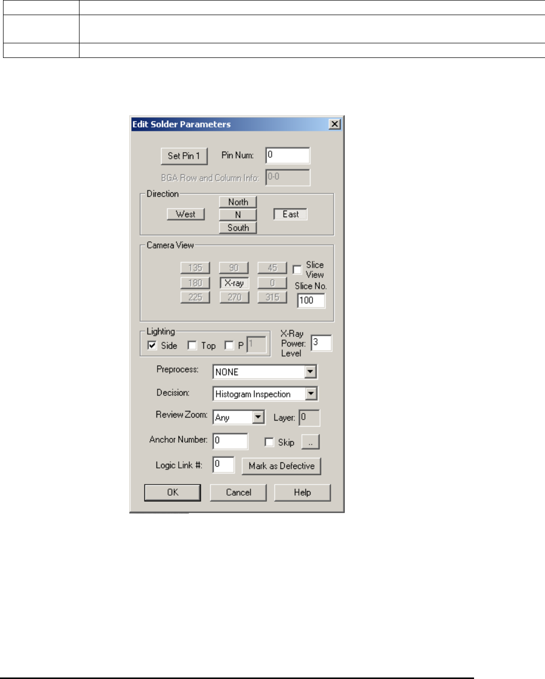
10.4.1 Edit Solder Parameters
Select Edit Solder Params.. from the Solder pop-up menu to open the Edit Solder Parameters
dialog.
The Pin Number box defines the solder box’s pin number.
Press the Set Pin 1 button to set the pin numbers for all solder boxes using a counterclockwise
convention.
The rest of the buttons on the dialog set the Direction, Camera View, Slice View, Slice No. and
Lighting for the inspection. You can also select one preprocess and one decision algorithm for
the inspection.
10-24 General Inspection Methodology
Currently there are seven decision algorithms for the solder inspection box: Histogram
Inspection, Pattern Matching, BGA Analysis, BGA Pin Inspection, Solder Blob Analysis,
Percent Void Inspection, PTH Solder Analysis, Fusion Solder and Xray Solder Analysis.
BGA Analysis and BGA Pin Inspection are for BGA solder. See 10.5.3 Solder Inspection for
more details. Fusion Solder is for the M1 AOI System with RGB light. Solder Blob Analysis and
PTH Solder Analysis are through-hole inspection algorithms for Nordson YESTECH AOI
systems only. Fusion Solder and PTH Solder Analysis are not used for X-ray inspection. Percent
Void Inspection is for void detection of solder joints under X-ray. Xray Solder Analysis is for
Resistor solder under X-Ray inspection.
All solder inspection boxes can be anchored by a marking box. Refer to 14.4 Anchor Block
Fiducial and Local Fiducial on the functionality of anchors. The X-ray Power Level specifies
the current X-ray power level used for current solder inspection. The Skip checkbox records
whether to skip (don’t inspect) current solder or not.
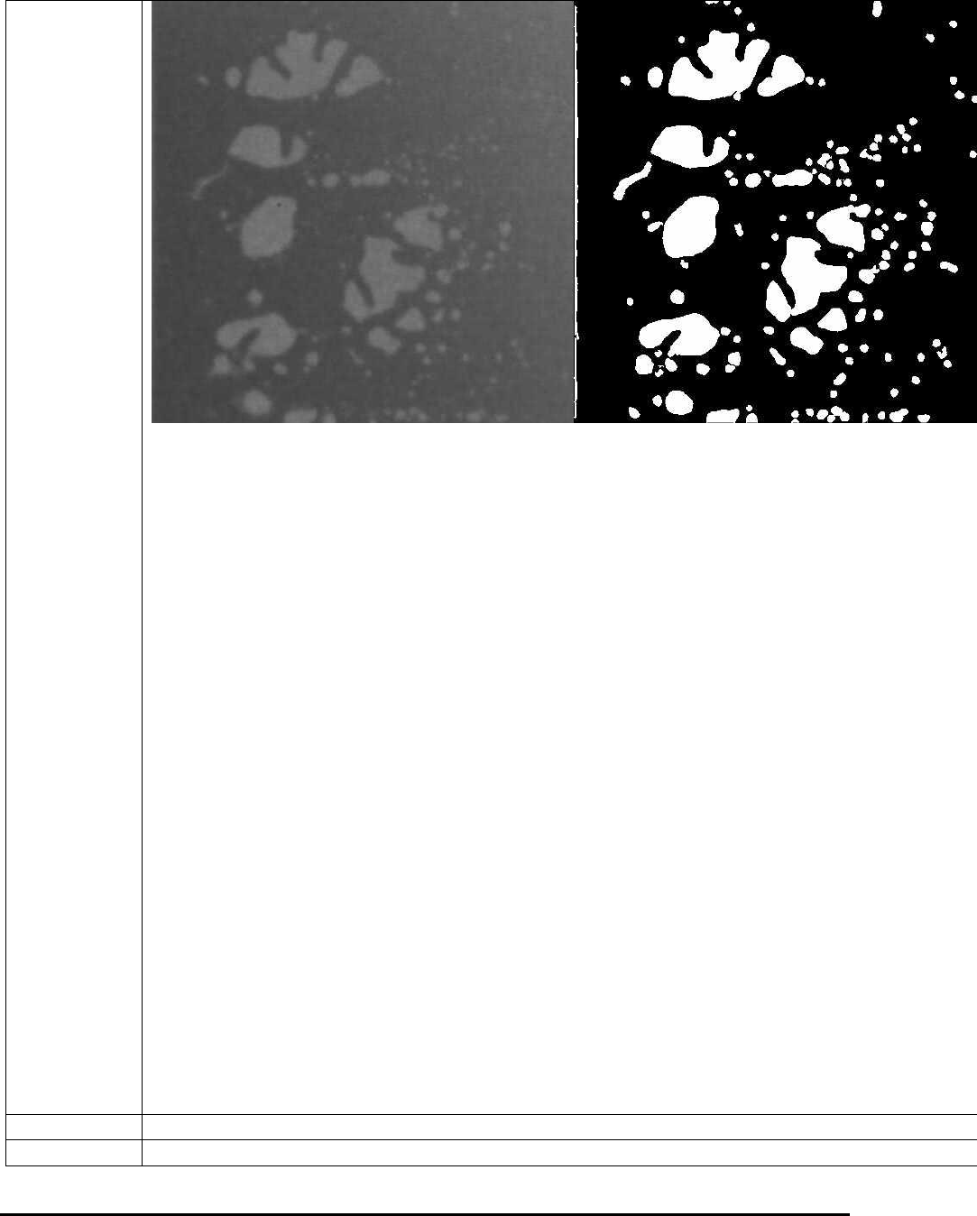
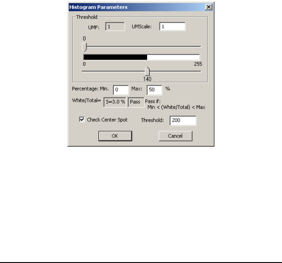
10.4.2 Histogram Parameters
Select Histogram Setup from the Solder pop-up menu to open the Histogram Parameters dialog.
Histogram inspection uses two threshold values to binarize the image into black or white pixels.
The algorithm then makes a decision based on the ratio between the two. The UMF and
UMScale are used for uniformity compensation which is disabled by default.
In X-ray view, histogram inspection can effectively detect insufficient or excess solder defects.