N7201A652E.pdf - 第248页
NPM- TT2 EJM1EE-MB -04O-03 Data editing 4-1-3 -1 D A B E Choose a recog nition mark. X[mm], Y[mm] D E A B If [Pattern] or [Group] is selected in the recognition mode and there are several types, cho ose the pattern numbe…
NPM-TT2 EJM1EE-MB-04O-03
4-1-2-2
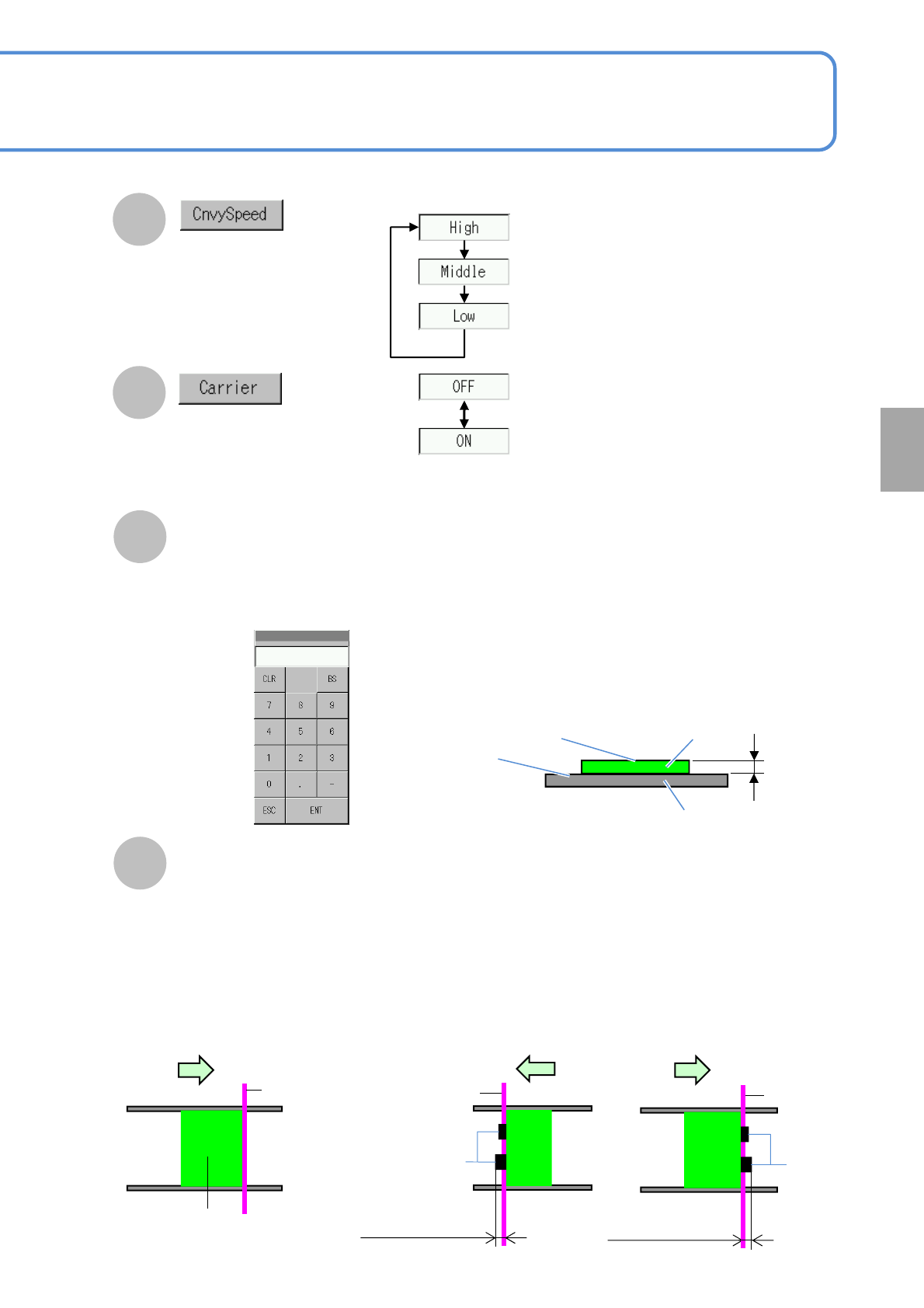
Choose whether to exist a carrier
PCB or not.
■Normal PCB positioning
■Placed component jutting out of PCB edges
PCB
Reference
Placed
components
Reference
Length of a placed
component jutting out (left)
G
Choose a PCB transfer
speed.
H
PCB flow direction
Placed
components
Reference
Length of a placed
component jutting out (Right)
PCB flow direction PCB flow direction
I
Touching the numerical part on the
screen opens the input window (See
below).
■When ’Yes’ selected
Height
●Enter the difference in height between a placement
surface and a clamp surface of the carrier PCB
when the carrier PCB is used. If the placement
surface is higher than the clamp surface, enter the
positive value, is it is lower, enter the negative
value.
Placement surface
Clamp surface
PCB
Carrier PCB
Height
●Height input (for positive value)
Setting
change
J
Jutting out Mount Length (Left, Right)
●If the placed component juts out from the PCB, the machine misjudges that the edge of the
placed component is the edge of the PCB, resulting in PCB recognition error.
So, entering the length of the jutting out placed component can carry out correct positioning.
●Enter max. length in cases where components already placed juts out of right or left PCB edges.
Input range : 0 to 9mm
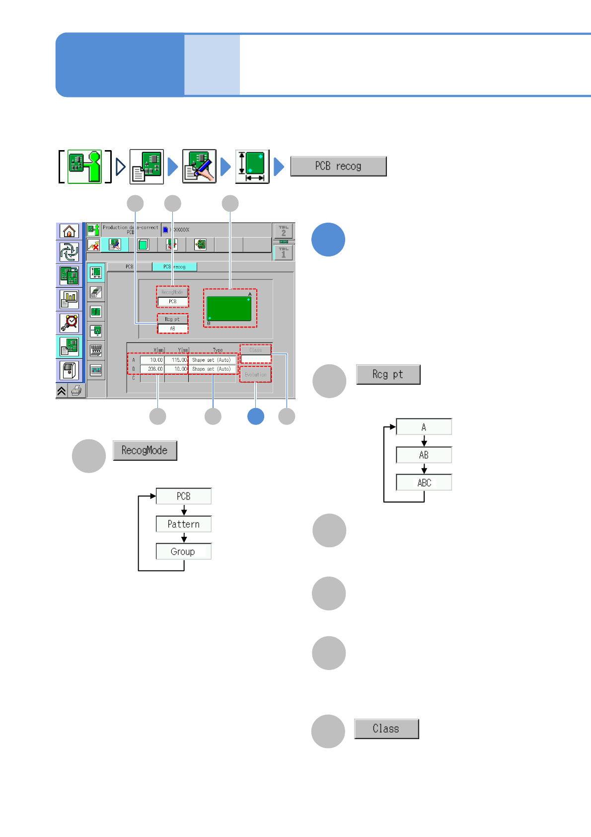
NPM-TT2 EJM1EE-MB-04O-03
Data
editing
4-1-3-1
D
A
B
E
Choose a recognition mark.
X[mm], Y[mm]
D E
AB
If [Pattern] or [Group] is selected in the
recognition mode and there are several
types, choose the pattern number or
group number.
F
1
Edit the data of the desired
field on the screen
Choose a recognition mode.
●PCB: Recognizes the recognition mark
●Pattern: Recognizes the pattern mark
●Group: Recognizes the group mark
PCB recognition data
edit 1
Describes how to edit the PCB recognition data registered by DGS.
Enter the PCB recognition coordinates
(X,Y) of each recognition mark.
●Touching the screen opens the input
window.
F
Type
The recognition method for each
recognition mark. Pressing the [Type]
field causes the shape setting screen of
each recognition mark to appear .
C
C
Illustration of a recognition mark (A or B or
ABC).
Recognition position on a PCB
3
Operating procedure
4-1-3
If ‘Panel Fiducial before Pattern/Pattern
Group Fiducials’ of Software Switch in DGS
is set, you can select only [Pattern] or
[Group].
NPM-TT2 EJM1EE-MB-04O-03
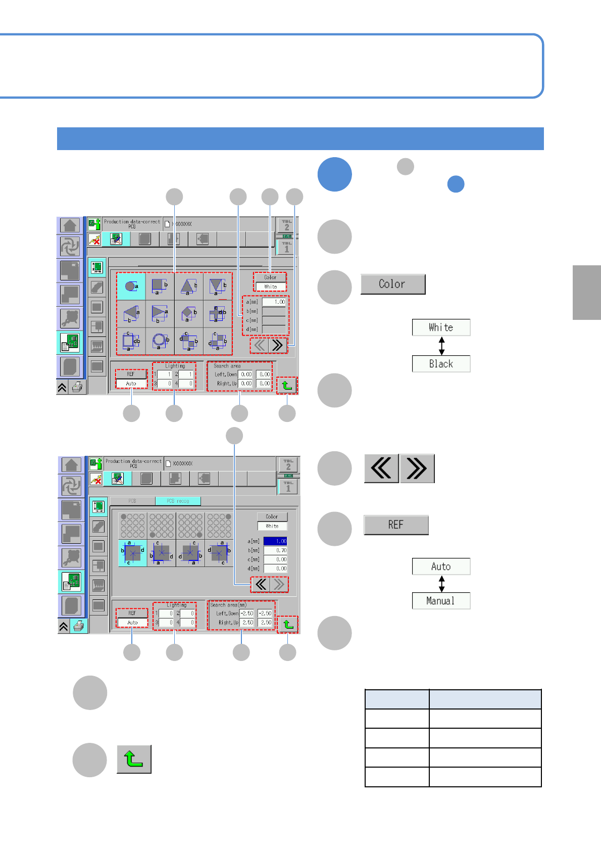
Lamp value of lamps 1 to 4.
4-1-3-2
B
A
C
D
Lighting
Size
Choose a recognition mark color.
E
Choose a light adjustment method.
F
Changes to the previous or next screen.
Shape selection
Search area
G
H
Returns to the previous screen.
Shape selection and edit
Size of a selected recognition mark
shape.
●Touching the screen opens the input
window.
Recognition range of one recognition mark.
●Touching the screen opens the input window.
Choose a recognition mark shape.
2
●Relationship between a head camera
lighting and lighting (→ P.5-3-9)
No. Type
1 Coaxial lighting
2 High angle lighting
3 Middle angle lighting
4 Low angle lighting
Setting
change
E F G
DA C B
H
E F G
D
H
Press (Type) on the
screen in step
(→P.4-1-3-1)
1
E