N7201A652E.pdf - 第360页
NPM- TT2 EJM1EE-MB-04 O-03 Produc- tion data teaching Bad mar k r ecognition teac h 2 4-2-10 -3 Operating procedure 4-2-10 5 5 5 6 ■ When the position and the size of recognition area are changed. 7 ■ When the threshold …
NPM-TT2 EJM1EE-MB-04O-03
4-2-10-2
Setting
change
1
2
Set a PCB on the PCB entrance
+
(The PCB is loaded onto the mount
stage, and the recognition camera
moves to the bad mark position)
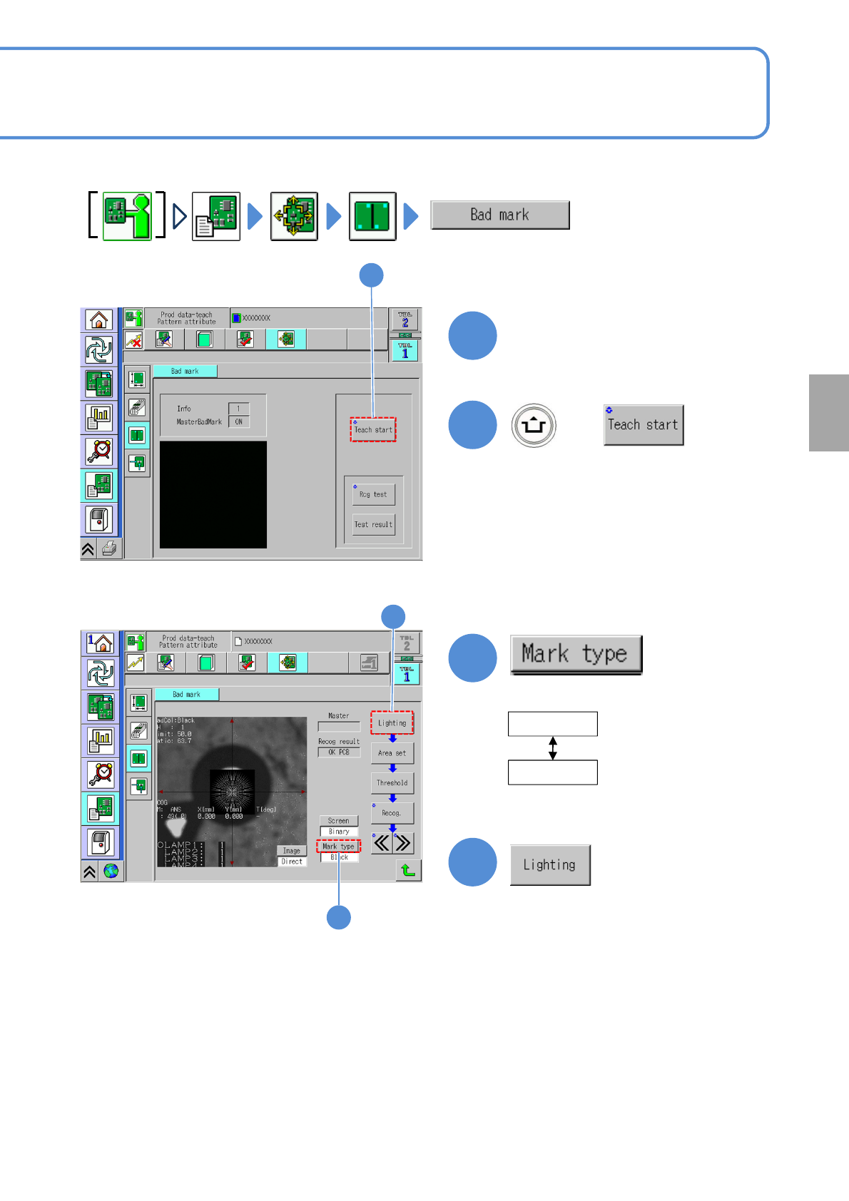
Describes how to check mark recognition when a bad mark exists on the PCB.
2
3
3
4
4
When the bad
mark is white
White
Black
●Select the mark type.
When the bad
mark is black
NPM-TT2 EJM1EE-MB-04O-03
Produc-
tion data
teaching
Bad mark recognition
teach 2
4-2-10-3
Operating procedure
4-2-10
5
5
5
6
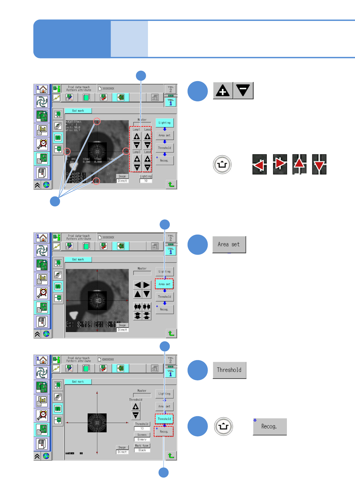
■When the position and the size of
recognition area are changed.
7
■When the threshold value being
recognized, screen switch or mark
type are changed.
6
8
7
+
8
After change
(Recognition is performed)
■If the bad mark is not located
near the center
●Align the cross line center to the
bad mark center.
+
●Adjust the brightness to obtain the
bad mark.
(→P.4-2-1 ‘How to adjust the lamp
value’)
NPM-TT2 EJM1EE-MB-04O-03
4-2-10-4
Setting
change
9
Confirm the recognition result
12
11
10
+
Confirm the message
●Choose the next bad mark.
●Displays in ‘Pattern’.
12
13
+
13
(The recognition result is displayed)
■For OK PCB
OK PCB
■For defect PCB
NG PCB
9
10 11