N7201A652E.pdf - 第505页
NPM- TT2 EJM1E E-MB-06O-04 6-1-8 -2 At a glance *1) C orrec table warpage by PCB wa rpage corr ection usin g the height s ensor, the c ross -section is a s ingle U type curve. For c omplex war page, using patter n warpag…
NPM-TT2 EJM1EE-MB-06O-04
Specifi-
cation
Operating procedure
6-1-8
6-1-8-1
Height sensor
Appearance
Applic
-able
PCB
*1)
PCB dimensions
PC size
300mm
transfer specifications
Dual lane mode
●Min: L 50 × W 50mm ●Max: L 510 × W 300mm
Single lane mode
●Min: L 50 × W 50mm ●Max: L 510 × W 590mm
PCB dimensions
M size 260mm
transfer specifications
Dual lane mode
●Min: L 50 × W 50mm ●Max: L 510 × W 260mm
Single lane mode
●Min: L 50 × W 50mm ●Max: L 510 × W 510mm
Thickness 1.6 to 8.0 mm
Material Glass epoxy
Measured surface
material
Copper foil + resist face, There should be area of at least 1.5
1.5mm on the copper foil and silk face.
The transparent and semi-transparent area are not target. (Glass
epoxy material face)
PCB warpage
amount
Upper warp: 2 mm or less, lower warp: 2 mm or less, and warp
gradient:0.5 % or less, The difference in height of an edge line
(transfer direction): 1 mm or less.
Function
Warpage toralrance
detection
If the measurement result exceeds tolerance, give a warning before
placement start. Also confirm the tolerance warp gradient (%).
Height control
Measures the PCB whole height (warpage) and control the
placement height.
Measured data
transfer
The data measured in the head machine in NPM-W is transferred
to the downstream machine.
The machine in downstream must be NPM-TT2. The data cannot
be sent to the machine other than NPM-TT2.
Regarding a PCB that the warpage shape varies each time it is
clamped, please consult us.
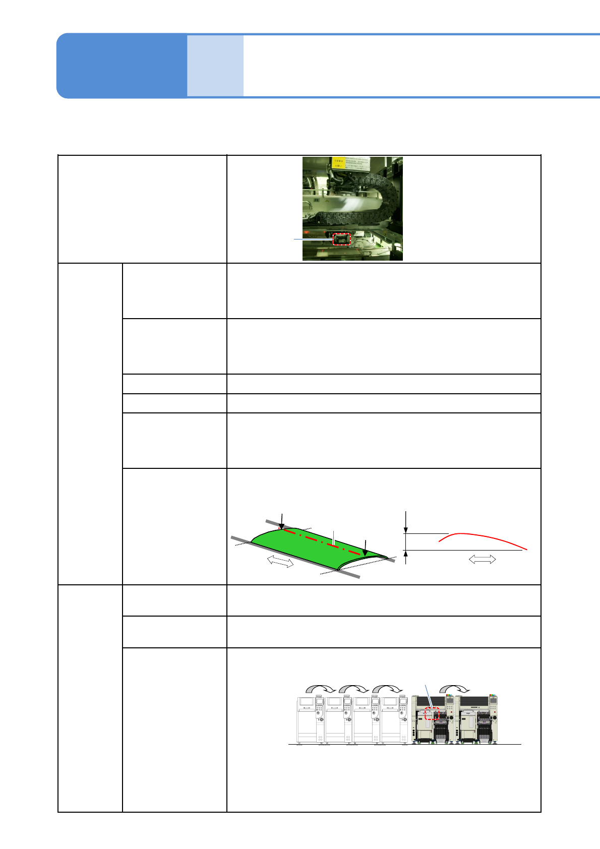
It controls the nozzle height when mounted by measuring the height (warpage) of the entire PCB.
If the measured result exceeds tolerance, give a warning before mount start to prevent the occurrence of PCB
quality defect.
A
B
B
A
Height sensor
NPM-D3 NPM-TT2
Edge line
Transfer direction
Transfer direction
1mmorless
Edge line
Height sensor
*2)
NPM-TT2 EJM1EE-MB-06O-04
6-1-8-2
At
a glance
*1) Correctable warpage by PCB warpage correction using the height sensor, the cross-section is a single U
type curve.
For complex warpage, using pattern warpage correction allows correcting a PCB as simple curve
combinations.
As for a PCB with slip (cutout) or thin PCB, warpage shape may be complex, so that we recommend to use
pattern warpage correction. (→■Pattern warpage correction)
*2) Choose the height sensor for the first NPM-TT2.
In single lane mode production, choose the sensor only for the front side, and in dual lane mode production,
choose the ones for both front and rear sides.
*3) For the maximum set number (total) of measuring points, see [6-1-1 Program data of machine specifications].
Measurement
condition
Height
PCB top surface ±4 mm (Area to be measured. It is not PCB warpage
tolerance)
Area Area of 5mm from PCB edge and cutout.
Points
*3)
Overall warpage correction : 9 points or more (up to 25 points/PCB)
Pattern warpage correction : 9 points/pattern or more (up to 25
points/pattern)
Measurement time
3.0 s (The value is under optimum condition when nine points on PCB
of 510 590 mm are measured)
■Pattern warpage correction
Warpage correction at measuring point per pattern is called pattern warpage correction (see below).
As for a PCB with slip (cutout), warpage shape may be complex and not be smooth (uniformed) curve.
In such a PCB, we recommend to use pattern warpage correction.
Slit
Pattern1 Pattern2 Pattern3
Pattern4 Pattern5 Pattern6
Measurement
point
A
A
Upward warpage
Downward
warpage
A – A cross section
●Correction impossible warpage shape
Ex. ) Waving PCB
NPM-TT2 EJM1EE-MB-06O-04
Specifi-
cation
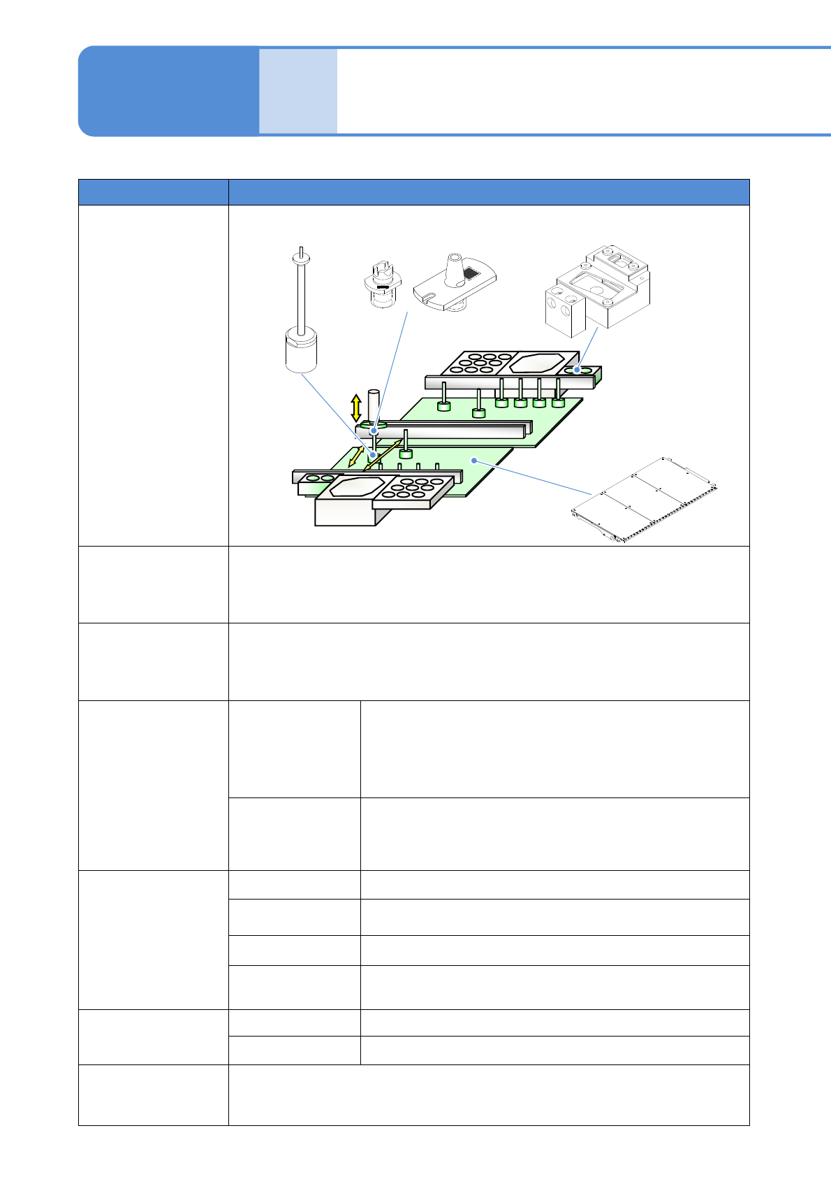
Support pin automatic
change 1
Operating procedure
6-1-9
6-1-9-1
Item Specification
Configuration
PCB dimensions
PC size
300mm
transfer specifications
Dual lane mode
●Min: L 50 × W 50mm ●Max: L 510 × W 300mm
Single lane mode
●Min: L 50 × W 50mm ●Max: L 510 × W 590mm
PCB dimensions
M size 260mm
transfer specifications
Dual lane mode
●Min: L 50 × W 50mm ●Max: L 510 × W 260mm
Single lane mode
●Min: L 50 × W 50mm ●Max: L 510 × W 510mm
Function
Data creation
function of the
support pin
arrangement
Checking the reverse side image downloaded to the DGS
window with the placement coordinates of the front side, the
machine visually decides the arrangement of support pins
and creates the production data.
●The data is created on DGS.
Support pin
automatic
arrangement
function
The support pins (for automatic change) are automatically
arranged using the nozzle for support pins based on the
production data.
Arrangement
conditions
Head
Placement head (8-/3-nozzle head)
Arrangement pitch
16mm pitch at minimum
The number of pins
30 pins at maximum/PCB
Arrangement data
Enables to create and choose the arrangement data per
machine
Applicable nozzle
100-nozzle
For 8-nozzle head
1100-nozzle
For 3-nozzle head
Arrangement time
90s/PCB
(350mm x 300mm The optimum condition value when 10 pins are arranged at the
center of the PCB)
Support pin
(for automatic change)
Nozzle for support pin
Nozzle changer
for support pin
PCB support block
(for automatic change)