N7201A652E.pdf - 第358页
NPM- TT2 EJM1EE-MB -04O-03 Produc- tion data teaching Bad mar k r ecognition teac h 1 4-2-10 -1 Operating procedure 4-2-10 Inputting the PCB data Inputting the pattern attribute data Starting the teaching Choosing the ba…
NPM-TT2 EJM1EE-MB-04O-03
3
Obtain origin offset by the
following steps
A
4
Confirm origin offset
A
Origin offset
(Origin offset obtained by teach is
displayed)
Setting
change
4-2-9-21
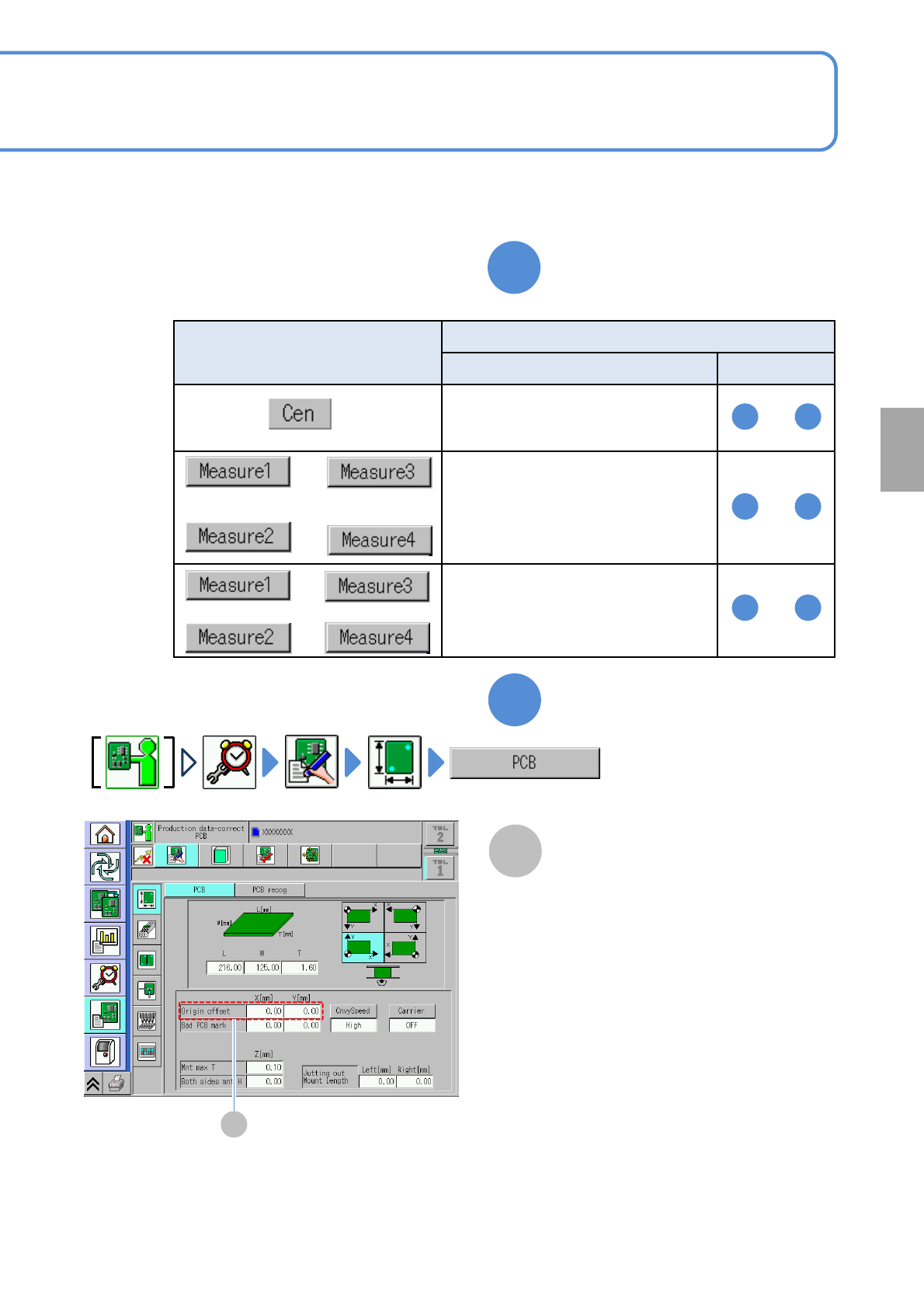
Measurement position
[Button name]
Process step
Section name Step
「Teaching with component
(measuring method: 1point)」
(→P.4-2-9-4 to P.4-2-9-7)
「Teaching with component
(measuring method: 2point)」
(→P.4-2-9-8 to P.4-2-9-12)
「Teaching with component
(measuring method: 1point)」
(→P.4-2-9-14 to P.4-2-9-15)
4 12
to
1 13
to
1 10
to
and
and
or
NPM-TT2 EJM1EE-MB-04O-03
Produc-
tion data
teaching
Bad mark recognition
teach 1
4-2-10-1
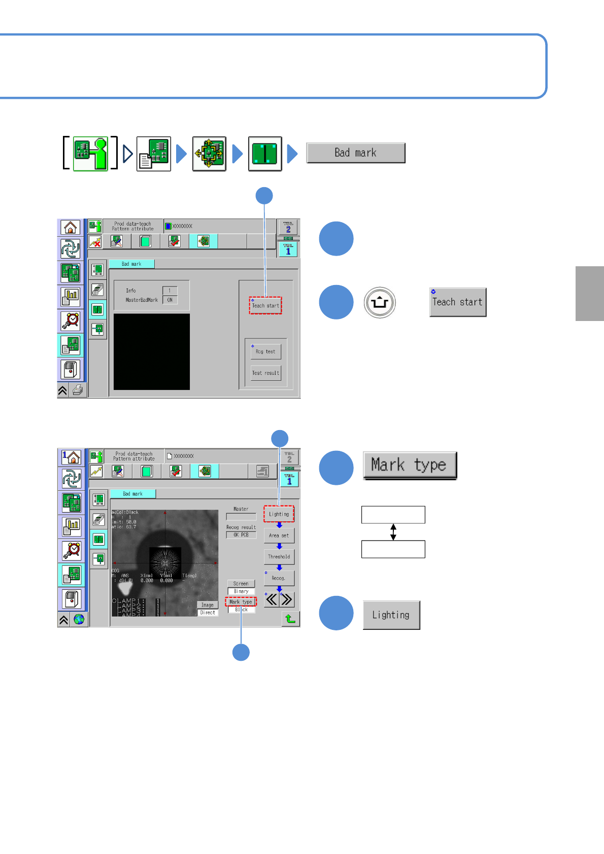
Operating procedure
4-2-10
Inputting the PCB data
Inputting the pattern attribute data
Starting the teaching
Choosing the bad mark
Setting the lamp values
Setting the area and threshold
Recognition
Saving data
To enable the bad mark recognition process, you need to turn ON the corresponding soft
switch.
Input the bad mark
position (coordinates).
Input the bad pattern
mark position
Created on
NPM-DGS.
Recognition Test
Teaching is complete.
When partial defect occurs in the produced PCB in the middle of the process, if a bad
mark is put on it, you can skip placement on that pattern.
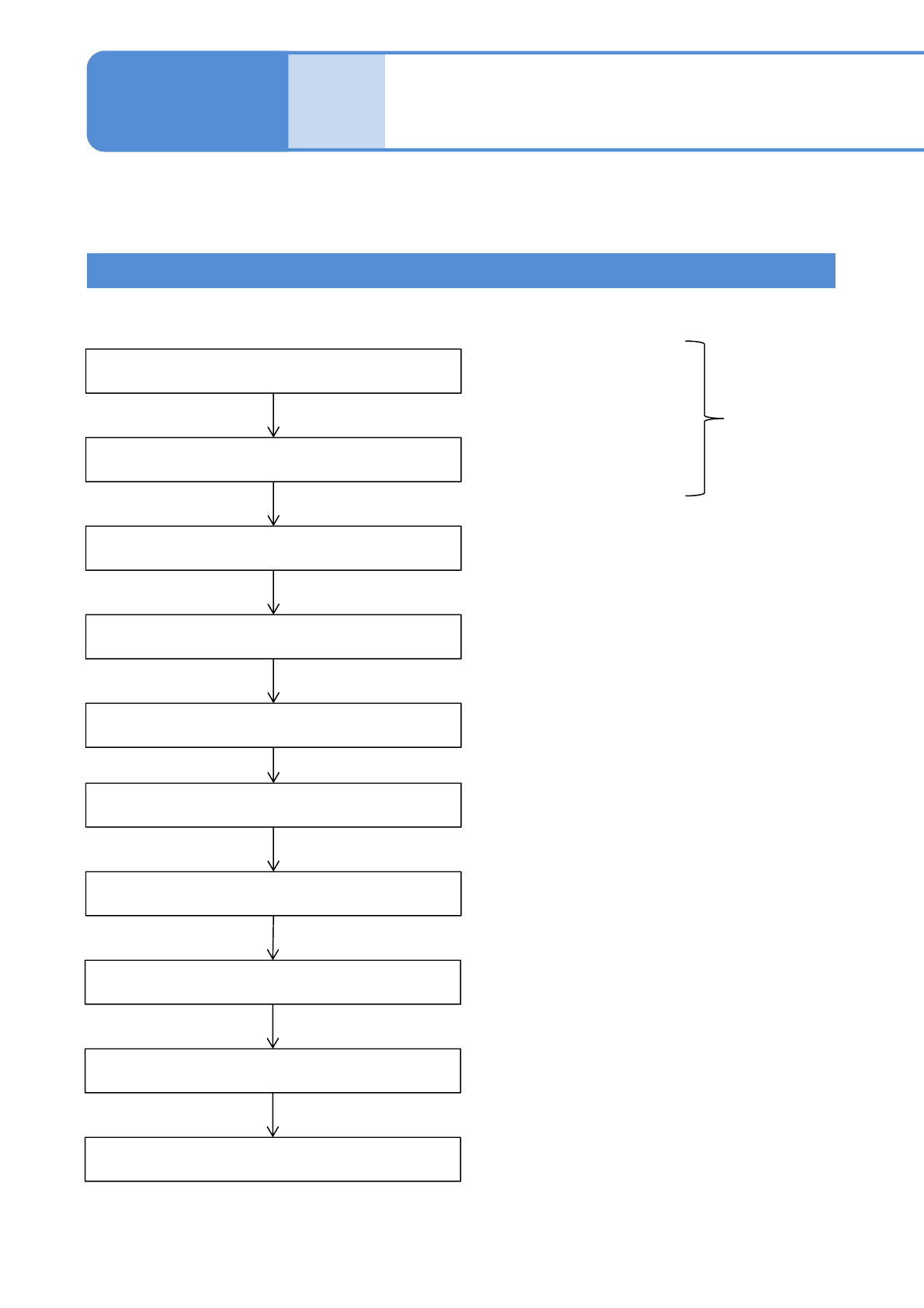
Teaching Flow
NPM-TT2 EJM1EE-MB-04O-03
4-2-10-2
Setting
change
1
2
Set a PCB on the PCB entrance
+
(The PCB is loaded onto the mount
stage, and the recognition camera
moves to the bad mark position)
Describes how to check mark recognition when a bad mark exists on the PCB.
2
3
3
4
4
When the bad
mark is white
White
Black
●Select the mark type.
When the bad
mark is black