1OM-1626-001_w.pdf - 第183页
1OM-1610 5-2 1. Specications : Chap.5 091 1-001 Item Description 7. Applicable PCB Mode Dual Transfer Mode Single Transfer Mode Dimensions X × Y 50 × 50 to 610 × 216 mm 50 × 50 to 610 × 381 mm Note : Four Corners : R1 t…
1OM-1610
5-1
1. Specications : Chap.5
0911-001
1. Specications
1.1 Specications of SIGMA-G4 Chip Mounter
Item Description
1. Model Name SIGMA-G4
2. Throughput
High-Speed Head Multi-Functional Head
65,000 CPH / module
Note :
The PCB transition time
under optimum conditions is
excluded.
Components : 9,000 CPH / 2 heads
Note :
The PCB transition time
under optimum conditions is
excluded.
3.
Placement
Accuracy
High-Speed Head Multi-Functional Head
0603 / 0402 : 40
µ
m (3
σ
) IC : 30
µ
m (3
σ
)
4.
PCB
T
ransition Time
0 second (Asynchronous Mode)
2 seconds or less (Synchronous Mode)
5.
Machine Scope This system employs the single side operation system and dual PCB transfer
system.
6. PCB Flow
Direction and
T
ransfer Reference
PCB Flow Direction
: From Left to Right / From Right to Left
(Selected when shipped from the factory)
Transfer Reference
: Front Left / Front Right
(Selected when shipped from the factory)
T1E1-1
1OM-1610
5-2
1. Specications : Chap.5
0911-001
Item Description
7. Applicable PCB
Mode Dual Transfer Mode Single Transfer Mode
Dimensions
X × Y
50 × 50 to 610 × 216 mm 50 × 50 to 610 × 381 mm
Note : Four Corners
: R1 to R1.5 mm
Tickness
0.5 to
5.0 mm
Mass
Max. 1.5
kg (50 <= X <= 260 mm)
Max. 2.5 kg (260 < X <= 610 mm)
Material
Glass Epoxy
Ceramic
(Option)
Notes :
(a) Consult
our marketing department or sales agency for
Glass Epoxy with light color.
(b) Depending on the PCB material, shape, warpage, mass
or surface condition (gloss), etc., it should be tested
whether or not the PCB can be transferred, or the
components can be placed normally, to conrm.
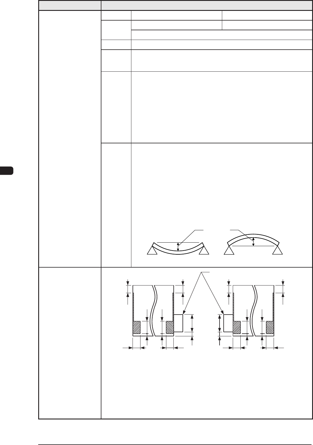
Warpage
0.2 mm
or less per 50 mm (unit length)
Upper : Max. 1.0 mm
Lower : Max. 1.0 mm
•
0.2 mm
or less per 50 mm (unit length)
Example
:
The
warpage must be 0.8 mm or less
when the
PCB size is 200 mm.
•
Max. 1.0
mm
Example
:
The
warpage must be 1.0 mm or less
when the
PCB size exceeds 250 mm.
Warpage
8. Limitation of
Cutout and Hole
on PCB
30.5
15
9
25
25
5
5
15
PCB Flow Direction
from Right to Left
15 15
30.5
15
9
25
25
5
5
15
PCB Flow Direction
from Left to Right
15 15
PCB Positioning Stopper
Unit : mm
Note :
The shadowed
areas show the areas where a cutout should not exist.
When a
cutout or a hole exists in the shadowed area, perform a PCB
positioning test and conrm that the PCB can be positioned normally.
T1E1-2
1OM-1610
5-3
1. Specications : Chap.5
0911-001
Item Description
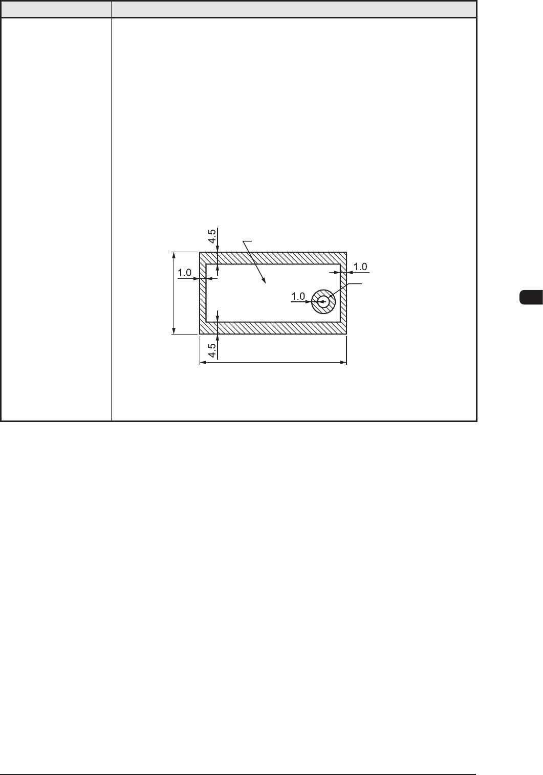
9. Correction Method
for PCB Location
PEC Recognition
•
By recognizing the ducial marks using the PEC camera, positional
deviation covering the whole area of PCB and expa
nsion of the printed
patterns on PCB can be corrected.
•
To correct the positional deviation covering the whole area of PCB,
ducial marks must be put on two or three places of PCB (Zones 1
through 5). Two ducial marks are required for each unit PCB of a
multi-unit PCB.
•
T
o correct the positional deviation of component placement points, put
one to two ducial marks on the PCB. In this case, it is recommended
that two ducial marks be located symmetrically such that the center
of gravity (the center of the ducial marks) becomes the center of the
component placement point.
(Front Side of Machine)
Range where a fiducial mark can be put
Hole, etc.
50.0 to 610.0
50.0 to 460.0
Unit : mm
T1E1-3