1OM-1626-001_w.pdf - 第206页
1OM-1610 5-25 1. Specications : Chap.5 (2) Material Copper Leaf, Nickel Plating, Solder Plating, Solder Leveler , Au Plating Note (a) A copper leaf, a resist, a coating, a silk print, and a punched hole should not exist…
1OM-1610
5-24
1. Specications : Chap.5
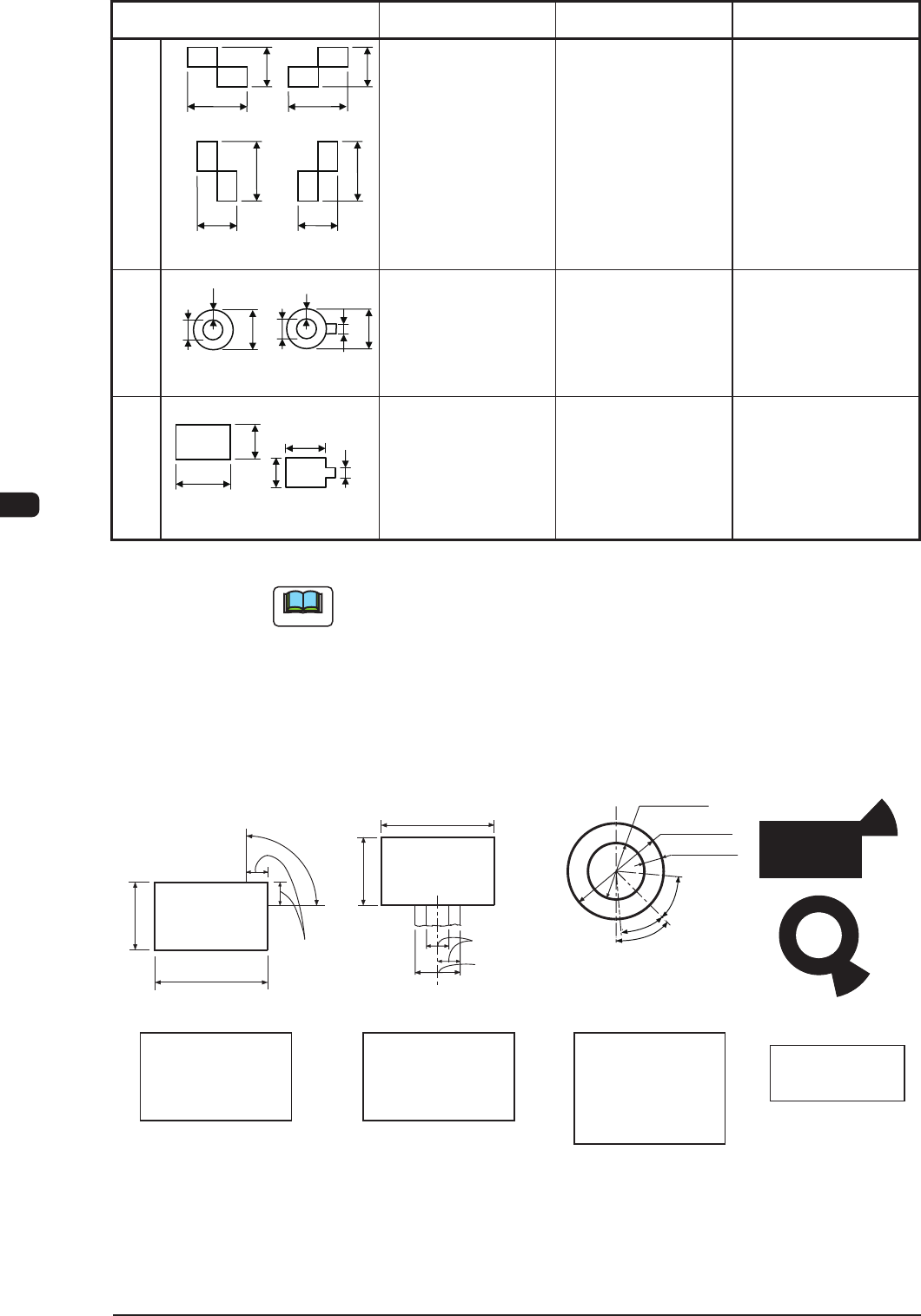
Mark Type D1 [mm] D2 [mm] Remarks
Checker
(Rectangle)
0.5 to 3.0 0.5 to 3.0
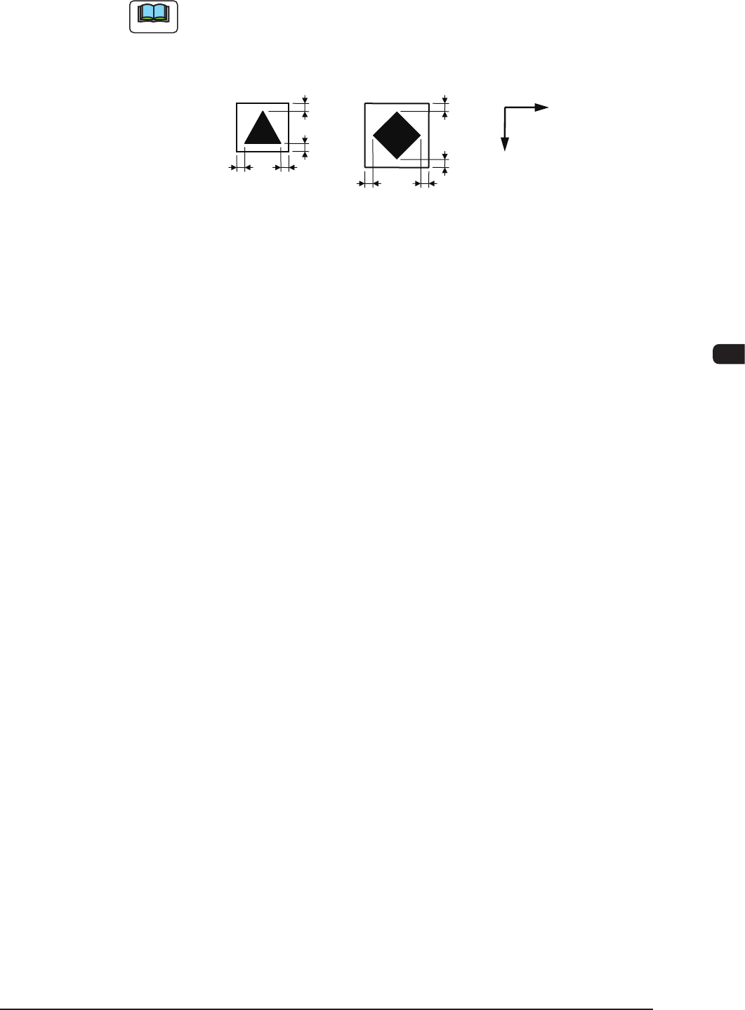
• Mark Reference :
Contact of Two
Rectangles
Through Hole
(Round)
0.5 to 3.0 0.5 to 1.5
• Mark Reference :
Center
• D2 :
Size of a punched
hole
• W : Min. 0.25 mm
Pad Mark
(Rectangular)
0.5 to 3.0 0.5 to 2.0
• Mark Reference :
Center of Gravity
D1
D2
D1
D2
D1
D2
D1
D2
Or Or
(Front Side of Machine)
D2
D1
W
(
Front Side of Machine
)
D2
W
D1
Note : b
(Front Side of Machine)
D2
D1
D1
D2
Note : b
T1E4-2
Note
(a) The error of the mark size should be within ± 10 % by comparison with the
reference pattern.
(b) A through hole or a pad mark should have only one land which is directed
in increments of 45°.
(2) Specications of Line extended from a Pad Mark or a Through Hole.
(See below)
1/3 of Side
Range of Tangent
Lines related between
Pad Mark and Land
(Front Side of Machine)
(Front Side of Machine)
0.5 to 2.0
0.5 to 3.0
0.5 to 2.0
0.5 to 3.0
Range of Tangent
Lines related between
Pad Mark and Land
(Front Side of Machine)
(Range of Tangent
Lines related between
Pad Mark and Land)
(Front Side of Machine)
0.5 to 1.5
1.0 to 3.0
45°
Examples of
Land Locations
Range of Land
Location for
Through Hole
(45° at the bottom
right of the hole)
Range of Land
Location in
Increments of 90°
for Pad Mark
Range of Land
Location in
Increments of 45°
for Pad Mark
Min. 0.25
40°
1/3 of Side
40°
Unit : mm
F1E3
0911-001
1OM-1610
5-25
1. Specications : Chap.5
(2) Material
Copper Leaf, Nickel Plating, Solder Plating, Solder Leveler, Au Plating
Note
(a) A copper leaf, a resist, a coating, a silk print, and a punched hole should not
exist in the range of 1.0 mm in both X and Y directions from the outermost
edges of a ducial mark. They may cause false recognition.
(Front Side of Machine)
1.0
X
Y
1.0
1.0
1.0
1.01.0
1.0
1.0
Example:
Unit : mm
F1E4
(b) The shape of PCB (a cutout, a punched hole), the external elements (light
reected from a structure, light emitted from an external device, etc.) may
sometimes interfere with the recognition of ducial marks.
(c) A ducial mark should make ample contrast with the surroundings. (To
prevent false recognition)
(d) Anything resembling a pattern similar to a ducial mark should not exist in
the designated window. If one exists, it may cause false recognition.
(e) A test may be required when the ducial mark cannot be recognized
because of the extreme warpage of the PCB.
0911-001
1OM-1610
5-26
2. List of Vacuum Nozzle Types : Chap.5
2. List of Vacuum Nozzle Types
The machine is equipped with nozzles designated in the delivery specications at
shipment.
Nozzle
Type
No.
Shape
Note (a)
Component Size
(mm)
Note (b)
Applicable Components
for Reference
Remarks
(
Part No.
Part Name
)
HA04A
2.5
s
1.6 to 4.0
s
3.0
Thickness
0.45 to 2.5
3216- and 3225-Type
Capacitors and Resistors,
Tantalum Capacitor A,
Mini-Mold Transistors
v
Nozzle for Front
Lighting
Recognition
I. D.
1.1
O. D.
1.8
HA05A
4.5
s
2.5 to 8.0
s
8.0
Thickness
1.0 to 6.5
4532-Type or Larger
Capacitors and Resistors,
Tantalum Capacitors
B, C, and D,
Aluminum Electrolytic
Capacitors,
SOP
6 to 10 pins
v
Nozzle for Front
Lighting
Recognition
I. D.
2.0
O. D.
3.0
HA09A
8.0
s
8.0 to
19.8
s
19.8
Thickness
1.0 to 5.0
SOP
QFP
PLCC
v
Nozzle for Front
Lighting
Recognition
I. D.
4.5
O. D.
6.0
HA11A
0.4
s
0.2
Thickness
0.1 to 0.2
0402-Type Capacitors and
Resistors
v
Nozzle for Front
Lighting
Recognition
I. D.
0.15
O. D.
0.5x0.3
HB03A
v
V-Grooved
2
s F
1.0 to
3.5 to
F
1.
5
Cylindrical Resistors and
Diodes
2.0
s F
1.0
2.0
s F
1.25
3
.
5
s F
1.4
v
Nozzle for Front
Lighting
Recognition
T1E5-1
0911-001