IPC-7095C-2013.pdf - 第113页
Most SMT joints have voids (under foot, plus inside/toe/ heel fillets). The majority are between 5 to 20 area percent voids with a small amount at 0% or around 25%. T ypical BGA solder joints average ~10 area percent, wit…
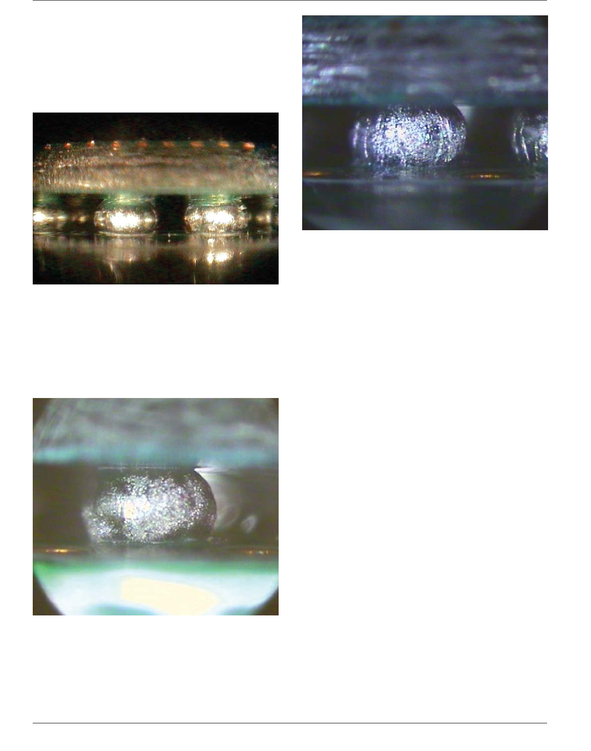
this technology is the inability to view interior rows with
the same level of quality and clarity. It is sometimes pos-
sible to focus on interior solder joints but not at the same
level of detail as the exterior rows. It is usually not possible
to see paste on the second or third row of balls. The anal-
ogy would be the inability to see trees in the center of a
forest from the outside.
Lens design is a distinguishing feature of this technology.
The highly advanced lenses are able to focus and redirect
an image 90° using a mirror or prism. A high-resolution
CCD camera and monitor are used to capture and display
the image. Magnification, depending on working distance,
ranges from 50x to 200x (see Figures 7-35 and 7-36).
Lighting is a critical factor. The image quality will be poor
if the light source does not properly illuminate the solder
joint being inspected. Front lighting permits frontal inspec-
tion of a solder joint while back lighting is useful for
detecting solder shorts and other obstructions. Back light-
ing also displays the solder joint outline which makes it
easy to view the overall shape.
A robust positioning system that provides adequate support
and protection for the lens and CCD camera is essential. It
must eliminate motion due to shock and vibration and it
must be adjustable through the desired range of motion.
Analytical software is also desirable. In addition to display-
ing a real time image of the solder joint it is useful to have
features such as image capture and measurement. Some
systems provide reference photographs of acceptable and
unacceptable solder joints. These images can be compared
simultaneously with the image being evaluated, which
reduces subjectivity during inspection.
7.3.7.1 Protocols for BGA Assembly Reliability and
mechanical strength of SMT joints are very important,
especially in high reliability applications. Voids and other
defects may hurt thermal cycle reliability. However, there
is temperature cycling data that exhibit voids, improving
the test results.
Voids in solder joints are common and unavoidable at low
levels. Voids in BGAs are very difficult to characterize
quantitatively, nondestructively. X-ray is the only practical
solution, but it’s tricky!
Void quality protocols must apply to all assembly situa-
tions. Rework, even when ‘‘required,’’ can make matters
worse. In-process and lot-acceptance protocols must be
developed. Out-sourcing/extended supply-chains pose
additional challenges.
Several early studies document the inevitable occurrence of
voids. Testing included some void characterization of con-
ventional SMT joints, as well as an objective to link abnor-
mal failures to abnormal causes, (e.g., extreme voids).
Figure 7-34 Endoscope Example
Figure 7-35 Lead-Free 1.27 mm Pitch BGA Reflowed in
Nitrogen and Washed Between SMT Passes
Figure 7-36 Lead-Free BGA Reflowed in Air and Washed
Between SMT Passes
IPC-7095C January 2013
98
Copyright IPC-Association Connecting Electronics Industries
Provided by IHS under license with IPC
Not for Resale
No reproduction or networking permitted without license from IHS
--`,,```,,,,````-`-`,,`,,`,`,,`---
Most SMT joints have voids (under foot, plus inside/toe/
heel fillets). The majority are between 5 to 20 area percent
voids with a small amount at 0% or around 25%. Typical
BGA solder joints average ~10 area percent, with some
averages as low as 5% and others in the 15% range. Within
the BGA the joints had different area percent voids ranging
from 0% to 35%.
Early-fail SMT joints do not have more voids than later-fail
joints. This is based on hundreds of comparisons of sym-
metrical parts: the ‘‘first-fail’’ joint does not have a larger
area percent void than the ‘‘last-fail’’ joint. Strong data
shows that variations in normal levels of voids are not
linked to thermal cycle life.
Methods (x-ray and fracture plane visuals) are approxi-
mately equivalent but both are very limited, difficult, or
subjective. One analysis compared void content of several
styles of early-fail BGAs vs. void content of equivalent
later-fail BGAs. No correlation was found. Early and late
failures had the same void content.
Note that all this BGA data involved ‘‘all-ball nets.’’ No
data exists to statistically link ‘‘first-fail joint’’ of a BGA to
its life. Therefore there is no numerical correlation of life
vs. void percentage. No data was taken that would be good
enough to establish trends within the 5-10 accuracy that
might be useful.
At this time, there is no new data that would establish a
numerical link (voids vs. life) for any/all of the component
types, under any/all conditions. Some information suggests
that normal voids variations are:
• For in-process control, use >35% area percent as the
threshold with a >50% void diameter threshold
• For reject/rework, use >45% area percent as the criteria
with a >65% void diameter threshold
7.3.7.2 Cracked Peripheral Interconnect Determina-
tions
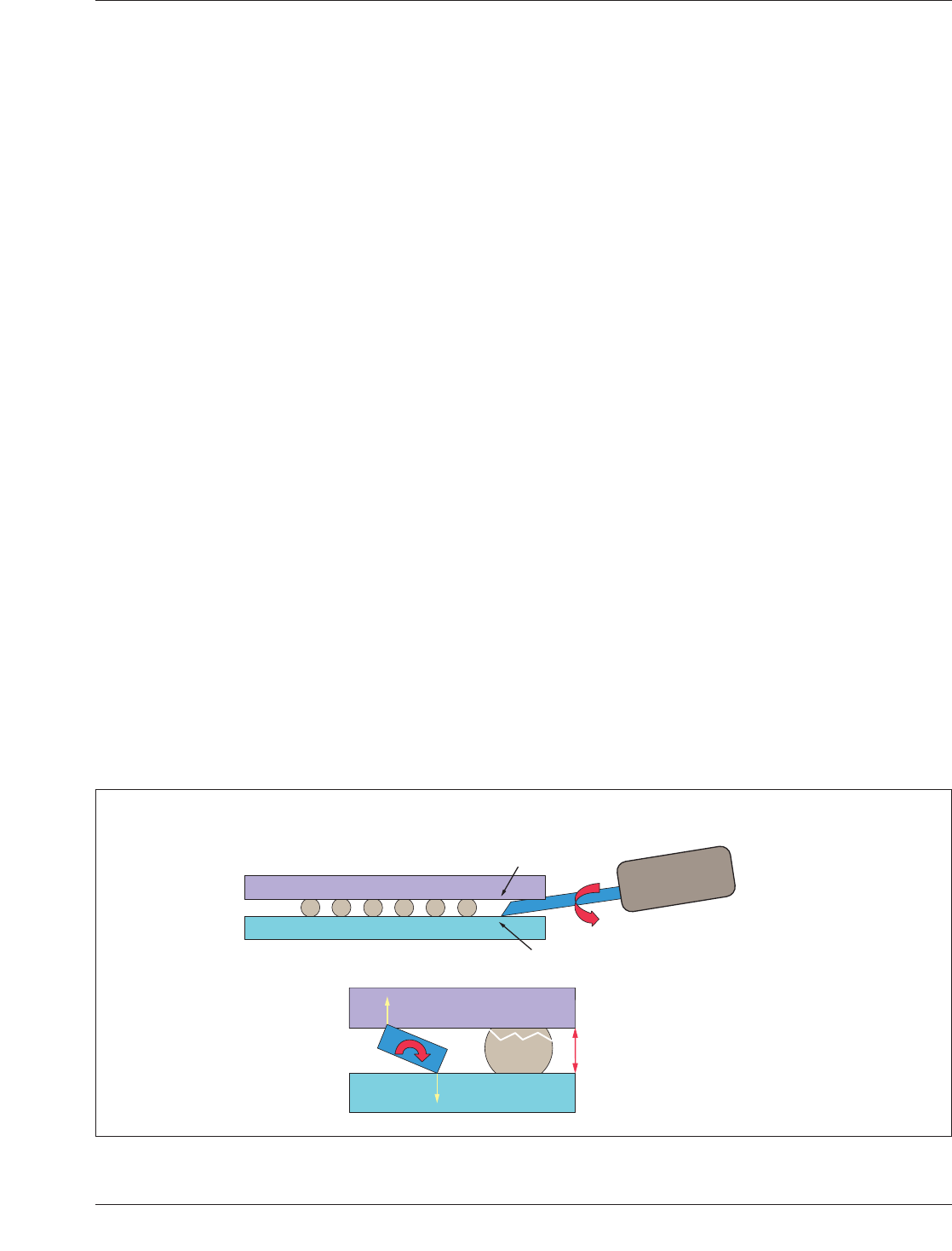
A torque-limited screwdriver can be used to identify
cracked peripheral interconnects (solder joints). Applying a
small force between the component and substrate will sepa-
rate fractured surfaces, as shown in Figure 7-37. This tech-
nique can identify open connections in a nondestructive
manner, and can determine if an open is due to a lifted
land, interfacial structure or bulk solder structure. This
technique does not work on some substrates, typically
those of low thickness laminates which produce a more
flexible component substrate (interposer).
7.3.8 Destructive Analysis Methods If nondestructive
methods fail to identify the cause of an anomaly, it may be
necessary to use destructive methods to isolate the problem
area. Such techniques will render the analyzed assembly
unusable. Once the cause of the failure has been identified
the information can be used to implement corrective
actions to eliminate the problem.
7.3.8.1 Cross-Sectioning Cross-sectioning is a destruc-
tive analysis method which looks at a section of the com-
ponents, substrate and solder joints after cutting it apart.
The first step in cross-sectioning is to identify or make a
best guess regarding the area that needs to be examined. If
more than one area is suspect then it needs to be deter-
mined whether those areas can be accessed sequentially on
the same component. If not, then the areas will need to be
prioritized according to the possibility of finding the prob-
lem or more than one component will need to be analyzed.
Next, if the problem area is a part of a larger assembly, it
may need to be isolated into a small more manageable por-
tion by cutting it out of the larger assembly. Care should be
taken to ensure that the evidence is not altered or destroyed
during the cutting process.
IPC-7095c-7-37
Figure 7-37 Engineering Crack Evaluation Technique
B
A
Side View
B
A
End View
BGA
Torque Screwdriver set at ~ 0.02 Nm
~ 0.03 mm minimum gap
January 2013 IPC-7095C
99
Copyright IPC-Association Connecting Electronics Industries
Provided by IHS under license with IPC
Not for Resale
No reproduction or networking permitted without license from IHS
--`,,```,,,,````-`-`,,`,,`,`,,`---
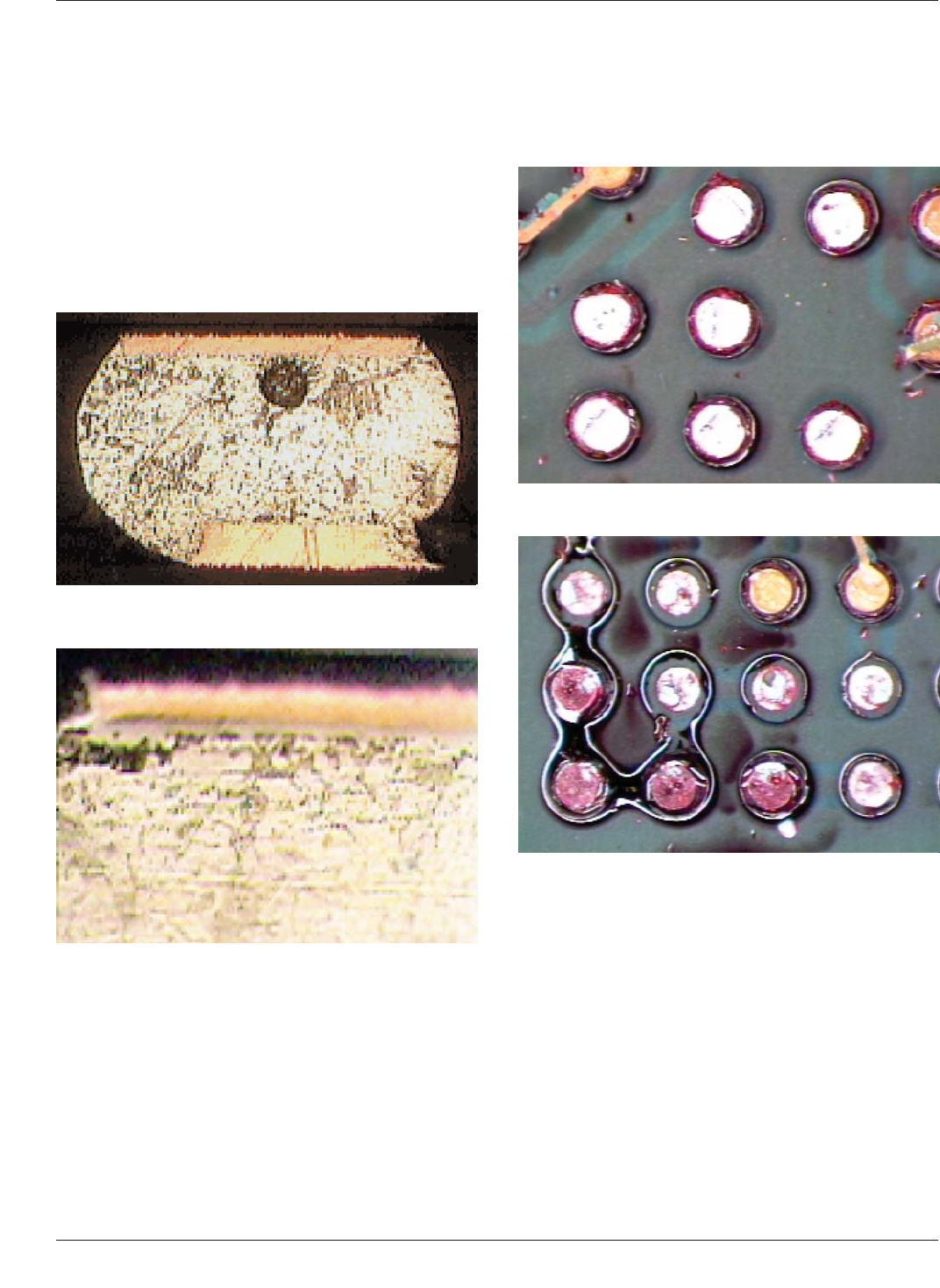
For proper sectioning, the sample should be molded in
resin to alleviate chipping or destruction of the sample dur-
ing cross-sectioning (see Figures 7-38 and 7-39). If fine
polishing of the area of interest is going to be required,
then the sample should be sectioned a reasonable distance
away from the interface of interest leaving sufficient dis-
tance for fine polishing of the interface.
In some cases, the entire component may need to be
ground through and looked at for the integrity of various
interfaces. A common failure analyzed through cross-
sectioning is an open occurring in an assembly. Such opens
may occur at the solder interface.
7.3.8.2 Dye Penetrant Dye penetrant methods can be
used during process set-up and in failure analysis to detect
solder joint cracking and wetting problems, and package
delamination. The sample is immersed in a low viscosity
liquid dye which penetrates any cracks, delaminated areas,
or open voids. The sample can then be peeled away and
examined for the presence of dye in the solder joints or at
material interfaces. If a fluorescent dye is used, the sample
is inspected under UV light. The dye enhances the visibil-
ity of flaws that might otherwise be difficult to detect. The
presence of dye on a solder land indicates poor wetting to
the land, and can be used to estimate the portion of the land
that was not wetted; however, very thin cracks may be so
small that liquids cannot completely enter because the sur-
face tension of the liquid will not allow it (see Figures 7-40
and 7-41).
7.4 Testing and Product Verification
7.4.1 Electrical Testing
Electrical testing is used to
evaluate the functionality of the electronic assembly. There
are two commonly used electrical test approaches:
in-circuit test (ICT) and functional test (FT).
ICT utilizes a dedicated bed-of-nails fixture to probe the
completed assembly. This test method is used to detect
faults caused by the manufacturing process and also to iso-
late the majority of nonfunctional components. The faults
found by ICT include solder bridge, solder open, compo-
nent mis-orientation, wrong component, component not
functional and conductor short.
Figure 7-38 A Solder Ball Cross Sectioned Through a Void
in the Solder Ball
Figure 7-39 Cross-Section of a Crack Initiation at the Ball/
Pad Interface
Figure 7-40 No Dye Penetration Under the Ball
Figure 7-41 Corner Balls have 80-100% Dye Penetration
Which Indicate a Crack
IPC-7095C January 2013
100
Copyright IPC-Association Connecting Electronics Industries
Provided by IHS under license with IPC
Not for Resale
No reproduction or networking permitted without license from IHS
--`,,```,,,,````-`-`,,`,,`,`,,`---