IPC-7095C-2013.pdf - 第73页
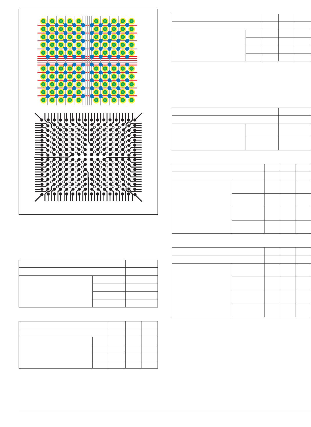
PCB: • Divide each BGA into four equal quadrants with lines parallel to the sides. From each quadrant, route conduc- tors and dogbones to escape vias from the BGA lands so that they go out radially from the BGA at 45 deg…
6.3.2 Surface Conductor Details Tables 6-5 through 6-7
shows various conductor routing characteristics for differ-
ent BGA pitches.
6.3.3 Dog Bone Through Via Details Tables 6-8 through
6-10 provide the details for conductor routing using the
dogbone via concept. The tables also are organized per via
pitch.
6.3.4 Design for Mechanical Strain Mechanical strain
and board flexure are major causes of PCB and BGA joint
damage. Several BGA layout strategies have been devel-
oped that can help reduce the impact of mechanical strain
on the BGA.
IPC-7095c-6-14
Figure 6-14 Conductor Routing Strategy
Table 6-5 Conductor Routing - 1.27 mm Pitch
Nominal Ball Diameter (mm) 0.75
Typical Solder Land Diameter (mm) 0.55
Conductor Spacing Width (µm) 150 2
125 2
100 3
75 4
Table 6-6 Conductor Routing - 1.0 mm Pitch
Nominal Ball Diameter (mm) 0.6 0.5 0.45
Typical Solder Land Diameter (mm) 0.45 0.40 0.35
Conductor Spacing Width (µm) 150 1 1 1
125 1 1 2
100 2 2 2
75333
Table 6-7 Conductor Routing - 0.8 mm Pitch
Nominal Ball Diameter (mm) 0.45 0.4 0.3
Typical Solder Land Diameter (mm) 0.35 0.3 0.25
Conductor Spacing Width (µm) 150 1 1 1
125 1 1 1
100 1 2 2
75123
Table 6-8 Conductor Routing - 1.27 mm Pitch
Nominal Ball Diameter (mm) 0.75
Typical Solder Land Diameter (mm) 0.55
Drill Diameter 0.35 mm
[0.0135 in]
Y
0.3 mm
[0.012 in]
Y
Table 6-9 Conductor Routing - 1.0 mm Pitch
Nominal Ball Diameter (mm) 0.6 0.5 0.45
Typical Solder Land Diameter (mm) 0.45 0.40 0.35
Drill Diameter 0.35 mm
[0.0135 in]
NNY
0.3 mm
[0.012 in]
NYY
0.25 mm
[0.010 in]
YYY
0.2 mm
[0.008 in]
YYY
Table 6-10 Conductor Routing - 0.8 mm Pitch
Nominal Ball Diameter (mm) 0.45 0.4 0.3
Typical Solder Land Diameter (mm) 0.35 0.3 0.25
Drill Diameter 0.35 mm
[0.0135 in]
NNN
0.3 mm
[0.012 in]
NNN
0.25 mm
[0.010 in]
NYY
0.2 mm
[0.008 in]
YYY
IPC-7095C January 2013
58
Copyright IPC-Association Connecting Electronics Industries
Provided by IHS under license with IPC
Not for Resale
No reproduction or networking permitted without license from IHS
--`,,```,,,,````-`-`,,`,,`,`,,`---
PCB:
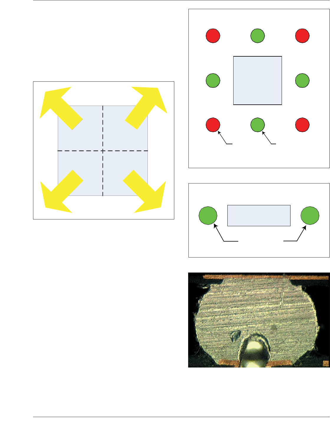
• Divide each BGA into four equal quadrants with lines
parallel to the sides. From each quadrant, route conduc-
tors and dogbones to escape vias from the BGA lands so
that they go out radially from the BGA at 45 degree
angles (see Figure 6-15). This increases the amount of
strain that corner lands can withstand before damage.
• Enlarge or teardrop the dogbones or routes to BGA cor-
ner lands.
PCA and Enclosures:
• Do not place screws near BGA corners in line with the
package diagonals (see Figure 6-16, red locations).
• Preferably place screws and bosses on the normal to the
midpoint of the BGA sides (see Figure 6-16, green loca-
tions).
• Use header connectors with a stiff body and provide PCA
support at both ends, especially for connectors with high
insertion and release forces (see Figure 6-17).
• Use washers under screw heads not larger than the boss
Outer Diameter to minimize torsional deformation of the
PCB.
6.3.5 Uncapped Via-in-Pad and Impact on Reliability
Issues
Via-in-pad (through-hole via, capped on bottom of
the board) for BGA lands can cause voids in the BGA
solder joints, which may impact reliability. Current data
indicate that, for the standard 25-35 mm package with
0.75 mm balls, there is no reliability risk from voids.
Accelerated aging tests have been performed and the fail-
ure rate was statistically equivalent to standard dogbone
designs. An illustration of the problem is shown in Figures
6-18 and 6-19.
IPC-7095c-6-15
Figure 6-15 BGA Dogbone Land Pattern Preferred Direc-
tion for Conductor Routing
Dogbone
Direction
Dogbone
Direction
Dogbone
Direction
Dogbone
Direction
BGA
IPC-7095c-6-16
Figure 6-16 Preferred Screw and Support Placement
BGA
AVOID
CORNER
PLACEMENT
PREFERRED
PLACEMENT
SCREW AND SUPPORT PLACEMENT
IPC-7095c-6-17
Figure 6-17 Connector Screw Support Placement
CONNECTOR SCREW SUPPORT
PROVIDE END
CONNECTOR
SUPPORT ON PCB
Figure 6-18 Cross Section of 0.75 mm Ball with Via-in-
Pad Structure (Indent to the Upper Left of the Ball is an
Artifact.)
January 2013 IPC-7095C
59
Copyright IPC-Association Connecting Electronics Industries
Provided by IHS under license with IPC
Not for Resale
No reproduction or networking permitted without license from IHS
--`,,```,,,,````-`-`,,`,,`,`,,`---
Vias capped on one side can pose a variety of reliability
issues. Each issue should be evaluated for relevancy to the
specific environmental design criteria:
• the hole may be partially filled creating uneven stresses
• the void may utilize a sizable part of the connection area
reducing the structural support
• the void may reduce the thermal path
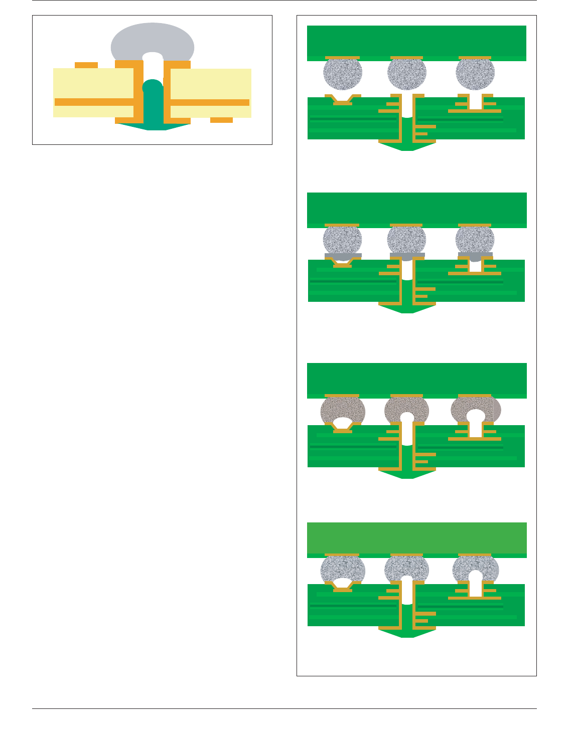
When using via-in-pad technology, a void will occur in the
joint as shown in Figure 6-19, unless the via is capped on
the component placement side of the board. Most experts
agree that these void conditions, created due to entrapped
air, are acceptable and have no impact on the reliability of
the joint. There is no doubt that the conditions depend not
only on the process, but the size of the BGA land and the
diameter of the hole. In addition, there is a difference as to
whether the hole is a through-hole, blind via, or microvia.
Figure 6-20 shows the characteristics of the three hole con-
figurations and what takes place at incoming after the sol-
der paste has been printed and the BGA has been placed;
the conditions of the ball and hole during reflow soldering;
and, finally, the characteristics of the resulting solder joint.
One of the major reasons for the occurrence of the void
conditions is the entrapped gas that exists under the solder
paste during the original paste printing and BGA place-
ment. During the reflow operation, the entrapped gas and
the solder paste volatiles need to escape, and this creates
the minor occurrences of absence of solder at the center
part of the ball as shown in the illustration.
6.3.6 Fine Pitch BGA Microvia in Pad Strategies When
the pitch is less than 0.8 mm, there is not enough room to
place a via using current mechanical drill technology for
full array BGA components. For finer pitch BGAs, in order
to achieve increased routing area, putting a microvia-in-pad
may be necessary. These are blind vias that connect to the
first or second internal layer of the printed board. They are
typically laser drilled but, in some cases, a mechanical
drilling process is used (see Figure 6-21).
IPC-7095c-6-19
Figure 6-19 Cross Section of Via-in-Pad Design Showing
Via Cap and Solder Ball
IPC-7095c-6-20
Figure 6-20 Via-in-Pad Process Descriptions
BGA
Incoming - Before Assembly Process
During Reflow Soldering
Post Reflow Soldering
After Solder Paste
Printing & BGA Placement
IPC-7095C January 2013
60
Copyright IPC-Association Connecting Electronics Industries
Provided by IHS under license with IPC
Not for Resale
No reproduction or networking permitted without license from IHS
--`,,```,,,,````-`-`,,`,,`,`,,`---