IPC-7095C-2013.pdf - 第148页
Hence, for better solder joint yields and solder joint reli- ability , the backward compatibility reflow soldering profile depicted in Figure 8-23 should be used. During this reflow profile, the SnAgCu solder ball also melts…
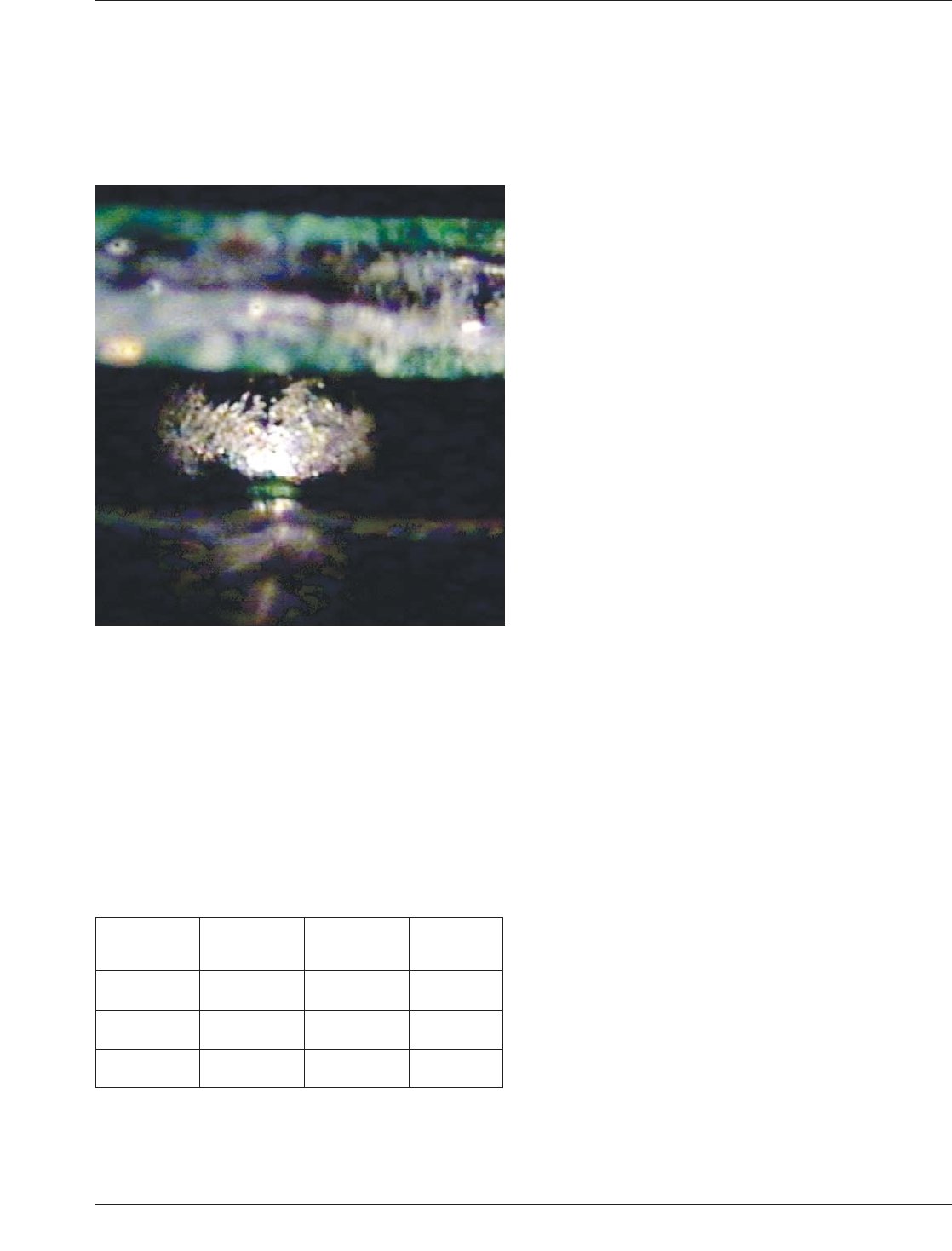
with the help of special microscopes such as the endo-
scope, peripheral solder joints can be viewed. SnAgCu sol-
der joint microstructures are multiphase microstructures
and the surface of the solder joints appears rough. Figure
8-22 shows a typical SnAgCu BGA solder joint. This is
much different from typical SnPb BGA solder joints which
usually have a shiny surface. Ball
8.5.5.6 Transition Lead-Free Technologies The transi-
tion from a total tin/lead soldering system to a total lead-
free soldering system is not going to happen overnight.
There may be an interim phase where tin/lead and lead-free
solders will co-exist on board assemblies. This transition
phase entails that the impact of lead in the SAC solder be
evaluated for impact on solder joint yields and reliability.
The likely lead-free board assemblies during this transition
phase are listed in Table 8-5.
The first possible lead-free board assembly listed above is
‘‘forward compatibility.’’ The board assembly soldering
process for forward compatibility assemblies has been con-
verted to lead-free technology with a change in the solder
paste composition and the reflow soldering profile to match
this change. However, some components, such as BGAs
that are soldered on the board, will still have tin/lead sol-
der due to the component supplier’s lead-free roadmap
having a conversion date later than the board assembler’s
conversion date. This results in the tin/lead solder joints of
the BGA-type components being ‘‘contaminated’’ by the
lead replacement metals in the lead-free solder paste.
The second possible lead-free board assembly listed above
is ‘‘backward compatibility.’’ Backward compatibility sce-
narios arise when component suppliers introduce the lead-
free components, but not all board assemblers that use
these components have converted their board assembly
lines to lead-free technology. These assemblers will still be
soldering the lead-free components with eutectic tin/lead
solder paste using tin/lead reflow soldering profiles. A tin/
lead component would obviously be preferable in this case,
but the component suppliers may, due to economic reasons,
not want to carry two component line items, one tin/lead
and one lead free, for the same device. The solder joints
formed with this combination of tin/lead solder paste and
lead-free solder ball will have a mixed composition. When
soldering a Ball Grid Array package with SnAgCu lead-
free solder balls using tin/lead solder paste, two different
scenarios arise based on the reflow profile used. The two
reflow profiles compared are shown in Figure 8-23 with the
total lead-free reflow profile also shown for comparison.
The tin/lead reflow profile, which is illustrative of the pro-
file used today for tin/lead assemblies, does not exceed the
melting point of the BGA’s SnAgCu solder ball. When a
reflow profile is unable to make lead-free solder ball melt
or dissolve, the solder joint yield and/or solder joint fatigue
life may suffer. The tin/lead solder paste deposited on the
lands of the solder balls melts but the SnAgCu solder balls
are still not molten. In such a material combination, the
lead may likely diffuse through the grain boundaries of the
solder ball. How high the lead from the tin/lead solder dif-
fuses up the SnAgCu solder ball will depend on how high
the reflow temperature gets and for how long the tin/lead
solder is molten. As shown in Figure 8-24, which depicts a
micrograph of a cross-section of a SnAgCu solder ball of a
BGA package soldered to a board using a reflow profile
which is unable to melt or dissolve SnAgCu solder ball, the
resulting solder joint microstructure is inhomogeneous.
This deleteriously impacts the solder joint reliability.
Yield impact on such solder joint is also deleterious due to
two reasons. One is due to the poor self-alignment of the
BGA during reflow soldering because the solder ball does
not become molten. This creates a potential for open joints
when the component is misaligned to some extent during
or after the Placement process step. Secondly, the lack of
‘‘ball collapse’’ may cause open solder joints from a lack of
contact between the solder paste deposit and the solder
ball.
Figure 8-22 Endoscope Photo of a SnAgCu BGA Solder
Ball
Table 8-5 Types of Lead-Free Assemblies Possible
Definition
Component
Termination/
BGA Ball Solder Paste
Board
Surface
Finish
Forward
compatibility
contains lead lead-free
leaded or
lead-free
Backward
compatibility
lead-free 63Sn37Pb
leaded or
lead-free
Total
lead-free
lead-free lead-free lead-free
January 2013 IPC-7095C
133
Copyright IPC-Association Connecting Electronics Industries
Provided by IHS under license with IPC
Not for Resale
No reproduction or networking permitted without license from IHS
--`,,```,,,,````-`-`,,`,,`,`,,`---
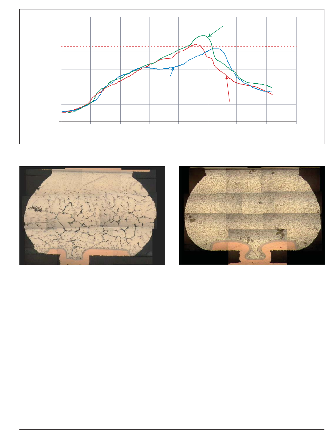
Hence, for better solder joint yields and solder joint reli-
ability, the backward compatibility reflow soldering profile
depicted in Figure 8-23 should be used. During this reflow
profile, the SnAgCu solder ball also melts, and lead from
the molten tin/lead solder paste mixes thoroughly with
molten SnAgCu solder ball and generates a homogeneous
structure of a lead-rich phase in the tin matrix. Such a
microstructure is shown in Figure 8-25.
Moreover, since the SnAgCu solder ball melts and col-
lapses, the self-aligning process and coplanarity reduction
also occur, thereby enhancing solder joint yields of the
BGA.
8.5.5.7 Ball Replacement Due to limited availability of
components with SnPb balls, some functional designs may
require ball replacement of the BGA component to allow
common processing with tin lead production assemblies.
This practice, while commonly employed, has drawbacks
due to the additional thermal cycles required for the ball
removal and subsequent replacement. Additionally, the
resulting interface alloy at the component to ball attach-
ment site may not achieve the desired or expected eutectic
properties. The process, however, does allow the use of
limited component types to comply with tin lead use strat-
egies for performance, contract mandates, and/or compat-
ibility with legacy or production designs that are suscep-
tible to the additional temperature excursion required for
lead free production processes. The sphere replacement
IPC-7095c-8-23
Figure 8-23 Comparison of Reflow Soldering Profiles for Tin/Lead, Backward Compatibility and Total Lead-Free Board
Assemblies
300
250
200
150
100
50
0
0
50
100
150 200 250
300
350 400
Tmelting for SnAgCu
Tmelting for SnPb
SnAgCu Balls do NOT Melt
Not good for backward compatibility
SnAgCu BAlls Melt
Will be OK for backward compatibility
Typical Lead Free Solder (SnAgCu) Profile
Temperature, Deg C
Time, Seconds
Figure 8-24 Micrograph of a cross-section of a BGA
SnAgCu solder ball, assembled onto a board with tin/lead
solder paste using the standard tin/lead reflow soldering
profile. The SnAgCu solder ball does not melt; black/grey
interconnecting fingers are lead-rich grain boundaries; rod
shape particles are Ag3Sn IMCs; grey particles are Cu6Sn5
IMCs.
Figure 8-25 Micrograph of a cross-section of a BGA
SnAgCu solder ball, assembled onto a board with tin/lead
solder paste using a backward compatibility reflows sol-
dering profile. The SnAgCu solder ball has melted.
IPC-7095C January 2013
134
Copyright IPC-Association Connecting Electronics Industries
Provided by IHS under license with IPC
Not for Resale
No reproduction or networking permitted without license from IHS
--`,,```,,,,````-`-`,,`,,`,`,,`---

process avoids paste alloy, PCB surface finish, and compo-
nent finish compatibility issues that can be very complex to
balance for successful production results.
Reballing of BGA components involves removal of the
original balls with a localized heat source such as a
vacuum desoldering tool, blade tip or solder wick. The
component surface is then cleaned and prepared for attach-
ment of new spheres that are located with a fixture that
aligns to the original pattern of the component. The spheres
are then attached to the component using a typical rework
heat source such as a convection reflow oven, or the fixture
with component and replacement spheres can be placed in
a reflow oven. As an alternate when many parts are to be
reballed, one can use automated laser systems that will pick
and place balls from a tray and then reflow them in place
on the BGA substrate using the laser beam.
In either case, the heat source must be controlled using a
thermal profile appropriate for the component and new ball
alloy. Once the balls are attached, the BGA package is
removed from the fixture and the balls can be examined
and cleaned in preparation for installation and soldering
with the remainder of the assembly components. As with
all BGA component processes, moisture and ESD sensitiv-
ity must be considered. BGA balls are commonly available
in a wide range of solder alloys and dimension but they
must be selected for compatibility with other process ele-
ments such as the board surface plating and solder paste. It
is also critical to maintain the component design spacing
and pitch through proper ball size and placement.
Detailed procedures for BGA Reballing are available in
IPC-7711/21B, ‘‘Rework, Modification and Repair of Elec-
tronic Assemblies.’’
8.6 Design for Reliability (DfR) Process As a general
recommendation, the Design for Reliability procedures
detailed in IPC-D-279 should be followed.
Appropriate DfR measures to improve reliability for grid
array components take one of two forms, which are best
employed in combination for improved reliability margins.
These measures are:
1. CTE-tailoring to reduce the global expansion mismatch.
2. Increasing attachment compliancy to accommodate the
global expansion mismatch by increasing the solder
joint height (stand-off).
3. Further, a DfR procedure aiming at high-reliability
could also include:
4. Eliminate the effect of the global expansion mismatch
by mechanically coupling the component and the sub-
strate with an appropriate underfill.
5. Choosing a soft die attach to reduce the impact of the
low CTE of the die (2.7 to 2.8 ppm/°C) on both the
global and local thermal expansion mismatch.
CTE-tailoring involves choosing the materials or material
combinations of the multilayer board and/or the compo-
nents to achieve an optimum CTE. An optimum CTE for
active components dissipating power is 1-3 ppm/°C
(depending on the power dissipated) with the multilayer
board having the larger CTE, and 0 ppm/°C for passive
components. Of course, since an assembly has a multitude
of components, full CTE optimization cannot be achieved
for all components—it needs to be for the components with
the largest threat to reliability. For military applications
with the requirement of hermetic and thus ceramic compo-
nents, CTE-tailoring has meant the CTE-constraining of
the multilayer boards with such materials as Kevlar™ and
graphite fibers, or copper-Invar-copper and copper-
molybdenum-copper planes. Such solutions are too expen-
sive for most commercial applications for which glass-
epoxy or glass-polyimide are the materials of choice for the
multilayer boards. Thus, CTE-tailoring has to take the form
of avoiding larger size components that are either ceramic
(CGAs, MCMs), plastic with Alloy 42 lead frames
(TSOPs, SOTs, or plastic with rigid bonded silicon die
(PBGAs).
Increasing attachment compliancy for leadless solder
attachments means increasing the solder joint height (C4,
C5, shimming, gluing, 10Sn90Pb balls, 10Sn90Pb col-
umns) or switching to a leaded attachment technology. For
leaded attachments, increasing lead compliancy can mean
changing component suppliers to those having lead geom-
etries promoting higher lead compliancy or switching to
fine-pitch technology.
The DfR process needs to emphasize a physics-of-failure
perspective without neglecting the statistical distribution of
failures. The process might involve the following steps:
• Identify Reliability Requirements – expected design life
and acceptable cumulative failure probability at the end
of this design life.
• Identify Loading Conditions – use environments (e.g.,
IPC-SM-785) and thermal gradients due to power dissipa-
tion, which may vary and produce large numbers of mini-
cycles (Energy Star).
• Identify/Select Assembly Architecture – part and substrate
selections, material properties (e.g., CTE), and attachment
geometry.
• Assess Reliability – determine reliability potential of the
designed assembly and compare to the reliability require-
ments using the approach shown here, a ‘‘Figure of
Merit’’ approach, or some other suitable technique; this
process may be iterative.
• Balance Performance, Cost and Reliability Requirements.
8.7 Validation and Qualification Tests Performance test
methods and qualification requirements are specified in
IPC-9701; IPC-9701A includes guidelines for lead-free
January 2013 IPC-7095C
135
Copyright IPC-Association Connecting Electronics Industries
Provided by IHS under license with IPC
Not for Resale
No reproduction or networking permitted without license from IHS
--`,,```,,,,````-`-`,,`,,`,`,,`---